Mastering FPGA design flow is crucial for various industries, including medical, transport, industrial, audio/video, space, and machine learning/computer vision. In order to excel in this field, it is important to have a comprehensive understanding of High-Level Synthesis (HLS), RTL (Register-Transfer Level) design, Synthesis, and Optimization, which are essential in FPGA design and verification processes.
High-Level Synthesis (HLS) in FPGA Design Flow
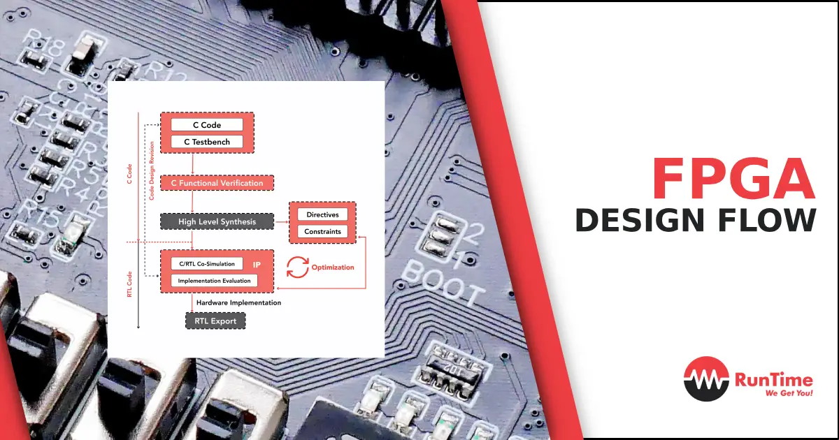
High-Level Synthesis (HLS) is a critical aspect of FPGA design flow. It refers to the process of translating high-level programming languages, such as C, C++, or SystemC, into hardware descriptions that can be implemented on Field-Programmable Gate Arrays (FPGAs). The primary purpose of HLS is to increase design productivity, reduce time-to-market, and enable designers to focus on algorithm development and optimization. HLS offers several advantages, including improved design abstraction, faster verification, and the ability to leverage existing software development tools and methodologies.
HLS Process
The HLS process starts with algorithm development, where designers create and refine the algorithm to be implemented on the FPGA. Next, an appropriate HLS tool is chosen for the task. These tools are responsible for converting high-level code into RTL (Register-Transfer Level) descriptions, which can be further synthesized into gate-level implementations.
Designers then code their algorithms in C, C++, or SystemC, utilizing HLS directives to guide the tool in generating efficient hardware. These directives can help optimize the design for area, performance, or power consumption, depending on the specific requirements of the project. Verification and debugging are essential steps in the HLS process, ensuring that the generated RTL design meets the functional requirements and performance goals.
HLS Optimization Techniques
Several optimization techniques can be applied during the HLS process to improve design efficiency. Some of the most common techniques include:
- Loop unrolling: This technique duplicates the loop body to reduce the number of loop iterations, thereby increasing throughput and reducing latency.
- Pipelining: By breaking the algorithm into smaller stages and processing multiple input data concurrently, pipelining can significantly increase the throughput of the design.
- Dataflow optimization: This involves analyzing and optimizing the data movement and storage within the design to minimize resource utilization and improve performance.
HLS Challenges and Limitations
While HLS offers many benefits, it also comes with some challenges and limitations. Some of these include:
- Resource constraints: Designers must balance the use of FPGA resources, such as logic elements and memory blocks, to achieve optimal performance without exceeding the available resources on the target FPGA device.
- Timing closure: Achieving timing closure, or meeting the required timing constraints, can be challenging in complex designs, particularly when using aggressive optimization techniques.
- Design complexity: As designs become more complex, it can be more challenging for designers to understand and manage the underlying hardware generated by the HLS tool, which may impact the overall FPGA design quality and verification process.
HLS is an essential aspect of FPGA design flow that offers numerous benefits in terms of design productivity and time-to-market. By understanding the HLS process, optimization techniques, and potential challenges, designers can effectively leverage HLS tools to create efficient and high-performance FPGA designs.
Register-Transfer Level (RTL) Design in FPGA Design Flow
Register-Transfer Level (RTL) design is a vital aspect of FPGA design flow. It refers to the process of creating a digital circuit design using a hardware description language (HDL) to define the data flow and the behavior of registers and combinational logic. RTL design plays a significant role in FPGA design, as it allows designers to specify and verify the functionality of their design before moving on to synthesis and optimization.
RTL Design Process
The RTL design process begins with the development of a functional specification, which provides a detailed description of the design’s intended behavior. Designers then use hardware description languages, such as VHDL or Verilog, to create an RTL representation of the design that captures both its data flow and control logic.
Once the RTL code is written, designers perform simulation and verification to ensure that the design behaves as intended and meets the specified performance goals. The RTL code is then synthesized, which involves transforming the RTL description into a gate-level representation that can be mapped to the target FPGA device.
RTL Optimization Techniques
During the RTL design process, several optimization techniques can be employed to improve the efficiency and performance of the design. Some of these techniques include:
- Combinational logic optimization: This technique involves simplifying the combinational logic in the design to reduce the number of gates and improve performance. This can be achieved by using Boolean algebra or other methods, such as Karnaugh maps and Quine-McCluskey minimization.
- Sequential logic optimization: By optimizing the state machines and flip-flop usage in the design, designers can reduce resource utilization and improve power efficiency. Techniques such as state encoding and state reduction can help achieve these goals.
- Hierarchical design: Organizing the design into a hierarchical structure can improve readability, modularity, and reuse of code. It also helps in managing the complexity of large designs and enables a more efficient verification process.
RTL design is an essential component of the FPGA design flow, as it allows designers to capture the intended functionality and performance of their designs before moving on to synthesis and optimization. By understanding the RTL design process and employing appropriate optimization techniques, designers can create efficient and high-performance FPGA designs that meet their specific project requirements.
Synthesis and Optimization in FPGA Design Flow
Synthesis is a crucial step in the FPGA design flow, as it plays a significant role in converting the RTL description of a digital circuit into a gate-level representation. This representation can then be implemented on an FPGA. To achieve an efficient design, optimization techniques are employed during the synthesis process, targeting area, timing, and power optimization.
Synthesis is defined as the process of transforming a Register-Transfer Level (RTL) design written in a hardware description language (HDL) into a gate-level netlist that can be mapped onto an FPGA. It is a critical step in the FPGA design flow, as it bridges the gap between the abstract RTL description and the physical implementation of the design.
Synthesis Process
The synthesis process consists of several stages, including:
- HDL code analysis: The synthesis tool analyzes the input RTL code to understand the design intent and identify the data flow and control logic.
- Logic optimization: At this stage, the synthesis tool applies various optimization techniques to minimize the size and complexity of the design while maintaining its functionality.
- Technology mapping: The optimized logic is then mapped to the target FPGA device’s specific resources, such as lookup tables (LUTs), flip-flops, and DSP blocks.
Synthesis Tools and Strategies
There are several synthesis tools and strategies available for FPGA designers, including:
- Vendor-specific tools: FPGA vendors often provide their own synthesis tools tailored for their devices, such as Xilinx’s Vivado and Intel’s Quartus.
- Third-party tools: Independent synthesis tools like Synopsys’ Synplify and Mentor Graphics’ Precision are available, which can support multiple FPGA vendors and devices.
- Custom scripts: Some designers choose to develop custom scripts to automate specific synthesis tasks or apply unique optimization techniques.
Optimization Techniques
Various optimization techniques can be applied during the synthesis process to improve the design’s efficiency. These techniques target different aspects of the design, such as:
- Area optimization: By minimizing the FPGA resources required for the design, area optimization can help reduce device utilization and lower the overall cost.
- Timing optimization: Ensuring that the design meets its timing requirements is crucial for proper functionality. Timing optimization techniques focus on improving the performance of critical paths and minimizing setup and hold time violations.
- Power optimization: Reducing power consumption is essential, particularly for battery-powered or thermally constrained applications. Power optimization techniques include clock gating, voltage scaling, and optimizing the switching activity in the design.
Verification and Validation
After the synthesis and optimization process, it is essential to verify and validate the design to ensure its correctness and adherence to the specified performance goals. This can be done through various methods, such as:
- Post-synthesis simulation: By simulating the gate-level netlist, designers can validate the synthesized design’s functional behavior and ensure that it matches the original RTL description.
- Static timing analysis: This technique helps designers identify and address any timing violations in the synthesized design, ensuring that the design meets its required performance targets.
- Formal verification: Using mathematical techniques, formal verification can prove the equivalence between the original RTL description and the synthesized gate-level netlist, providing a high level of confidence in the design’s correctness.
Conclusion
Synthesis and optimization are essential aspects of the FPGA design flow. By understanding the synthesis process, employing suitable tools and strategies, and applying appropriate optimization techniques, designers can create efficient and high-performance FPGA designs that meet their project requirements.
Hire the Best Engineers with RunTime Recruitment
Our expert team of engineers-turned-recruiters offers in-depth knowledge of technical recruiting in the engineering industry.
If your company is looking to recruit highly skilled engineers worldwide, contact us today and we will do the sourcing for you. Or if you’re an engineer looking for new opportunities, you can check RunTime Recruitment’s job site for job vacancies.


