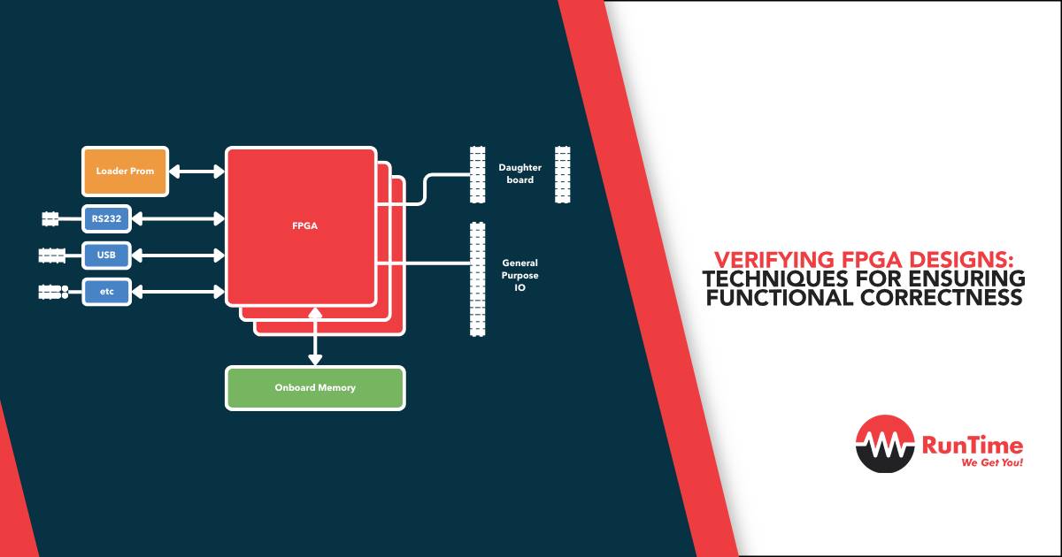
Field-Programmable Gate Arrays (FPGAs) are widely used in embedded systems due to their flexibility, performance, and scalability. Whether in telecommunications, aerospace, automotive, or AI applications, FPGAs allow engineers to implement complex designs. However, designing an FPGA is only half the battle—verification is where the design truly comes to life. Verification ensures functional correctness, detects design flaws, and prevents costly rework.
This article provides a comprehensive guide to verifying FPGA designs, including common challenges, verification methodologies, tools, and best practices for ensuring functional correctness. It is tailored for embedded engineers aiming to build robust and reliable FPGA-based systems.
Why Verification is Crucial for FPGA Designs
Verification is the process of ensuring that a design meets its specified requirements and behaves as intended. For FPGA designs, this involves verifying that the implemented logic matches the expected functionality and performs correctly under various operating conditions.
Key Goals of FPGA Verification
- Correctness: Validate that the design behaves as specified in the requirements.
- Timing Compliance: Ensure the design meets timing constraints to avoid metastability and timing violations.
- Robustness: Test the design under edge cases and corner conditions to ensure reliability.
- Debugging and Optimization: Identify and fix functional bugs while optimizing performance.
Consequences of Inadequate Verification
- Functional Failures: Misbehavior in real-world scenarios can cause system malfunctions.
- Cost Overruns: Debugging issues in deployed systems can be expensive and time-consuming.
- Delayed Time-to-Market: Verification bottlenecks can extend project timelines.
Challenges in Verifying FPGA Designs
- Complexity:
- Modern FPGAs integrate millions of logic gates, DSP blocks, and high-speed transceivers, increasing verification complexity.
- Concurrency:
- FPGA designs involve parallel processes, making it harder to debug and simulate compared to sequential software systems.
- Timing Issues:
- Ensuring that all signal paths meet timing constraints is critical but challenging, especially in high-frequency designs.
- Integration:
- Verifying interactions between multiple subsystems, such as interfaces, memory controllers, and custom logic, requires meticulous planning.
Verification Methodologies for FPGA Designs
1. Simulation-Based Verification
Simulation is the cornerstone of FPGA verification. It involves running a digital model of the design through testbenches to validate behavior.
Key Steps:
- Create a Testbench:
- Develop a test environment to drive inputs and monitor outputs of the design.
- Define Test Cases:
- Write test cases to cover typical, edge-case, and corner-case scenarios.
- Run Simulations:
- Use simulation tools like ModelSim, Xilinx Vivado Simulator, or QuestaSim.
Advantages:
- Detects functional errors early in the design cycle.
- Allows fine-grained observation of signals, registers, and internal states.
Best Practices:
- Use self-checking testbenches that automatically validate outputs against expected results.
- Employ waveform viewers to analyze signal interactions visually.
2. Formal Verification
Formal verification uses mathematical techniques to prove the correctness of a design.
How It Works:
- Tools like Synopsys VC Formal or JasperGold analyze the design to check for specific properties (e.g., assertions, state coverage).
- Commonly used for safety-critical systems where functional correctness is paramount.
Advantages:
- Exhaustive: Covers all possible input scenarios, unlike simulation, which is limited to specific test cases.
- Ideal for verifying small, critical modules like state machines or protocols.
Limitations:
- Computationally intensive for large designs.
- Requires expertise in formal methods and property definition.
3. Hardware-In-The-Loop (HIL) Verification
HIL verification involves testing the FPGA design on actual hardware while interfacing with real-world inputs and outputs.
How It Works:
- Load the synthesized design onto the FPGA.
- Connect the FPGA to a test rig or simulation environment that mimics real-world conditions.
Advantages:
- Verifies the design in its actual operating environment.
- Detects issues related to physical hardware, such as signal integrity or timing problems.
Best Practices:
- Use hardware debuggers like Xilinx Chipscope or Intel SignalTap to probe internal signals.
- Include test interfaces (e.g., UART or SPI) in the design for easy debugging.
4. Emulation
Emulation uses hardware accelerators to verify FPGA designs faster than traditional simulation.
How It Works:
- Map the design onto a larger, pre-verified FPGA or emulation platform (e.g., Cadence Palladium, Synopsys ZeBu).
- Run test scenarios to validate the design’s behavior.
Advantages:
- Faster than software-based simulation.
- Scales well for large, complex designs.
Limitations:
- High cost of emulation platforms.
- Requires additional effort to map the design to the emulator.
5. Timing Verification
Timing verification ensures that the design meets all timing constraints, avoiding race conditions and metastability.
Key Steps:
- Static Timing Analysis (STA):
- Use tools like Vivado or Quartus Prime to check setup and hold times, clock skew, and path delays.
- Post-Implementation Simulation:
- Validate timing after synthesis and placement.
Best Practices:
- Use constraints files (SDC/XDC) to define timing requirements.
- Optimize critical paths by restructuring logic or pipelining.
6. Code Coverage and Functional Coverage
Code and functional coverage measure how thoroughly your verification tests exercise the design.
Metrics:
- Code Coverage:
- Percentage of HDL lines executed during simulation.
- Functional Coverage:
- Verification of all intended functionality, such as FSM transitions or protocol compliance.
Tools:
- Use tools like VCS, QuestaSim, or Incisive for automated coverage analysis.
Best Practices:
- Aim for high coverage percentages (e.g., 90%+).
- Review uncovered areas to identify gaps in testing.
Best Practices for Effective FPGA Verification
- Start Verification Early:
- Begin testing at the module level before integrating the entire design.
- Automate Regression Testing:
- Use scripts or frameworks to rerun tests after every design change.
- Reuse Verification IPs (VIPs):
- Leverage pre-verified IPs for standard protocols like Ethernet or PCIe.
- Implement Assertions:
- Embed assertions in your code to monitor critical conditions during simulation.
- Version Control:
- Use tools like Git to track design and testbench changes systematically.
Common Verification Pitfalls and How to Avoid Them
1. Insufficient Test Coverage
Issue: Missing edge cases or corner scenarios. Solution: Use coverage metrics to guide additional test development.
2. Ignoring Timing Analysis
Issue: Functional simulations pass, but timing issues cause failures in hardware. Solution: Perform thorough static timing analysis and post-synthesis simulation.
3. Overlooking Integration Testing
Issue: Focusing only on individual modules without testing system-level interactions. Solution: Develop integration testbenches to verify subsystem interoperability.
4. Relying Solely on Simulation
Issue: Simulation misses real-world issues like signal integrity or power fluctuations. Solution: Complement simulations with HIL testing or physical hardware verification.
Case Study: Verifying an FPGA-Based Video Processing System
Scenario: A video processing system implemented on an FPGA needs verification for functional correctness and timing compliance.
Verification Approach:
- Simulation-Based Verification:
- Developed a testbench to simulate video input and validate processed output.
- Used waveform analysis to confirm pixel timing and frame synchronization.
- Formal Verification:
- Verified the correctness of the FIFO buffer and memory controller using property assertions.
- Hardware-In-The-Loop Testing:
- Loaded the design onto the FPGA and connected it to a real camera and display.
- Used an oscilloscope to verify signal integrity and timing.
- Timing Analysis:
- Performed static timing analysis to ensure compliance with 150 MHz clock constraints.
Outcome:
- The verification process identified and resolved critical bugs, such as incorrect color-space conversion and clock domain crossing issues.
- The system passed functional and timing tests, ensuring reliable operation in production.
Tools for FPGA Verification
- Simulation Tools:
- ModelSim, QuestaSim: For RTL simulation.
- Vivado Simulator: Integrated tool for Xilinx FPGAs.
- Formal Verification:
- JasperGold, VC Formal: Industry-standard formal analysis tools.
- HIL Tools:
- SignalTap, ChipScope: For hardware-level debugging.
- Timing Analysis:
- Vivado, Quartus Prime STA: For timing verification and optimization.
Conclusion
Verification is the backbone of reliable FPGA design. From simulation-based verification and formal methods to hardware-in-the-loop testing and timing analysis, each technique plays a critical role in ensuring functional correctness. By adopting a systematic and thorough approach to verification, embedded engineers can mitigate risks, reduce debugging time, and deliver robust FPGA designs that meet stringent performance and reliability standards.
Investing in effective verification practices not only prevents costly rework but also builds confidence in the quality of your embedded systems, enabling success in even the most demanding applications.


