In the rapidly evolving world of electronics, the demand for smaller, faster, and more efficient devices is driving innovation at every level of design. While much attention is given to advancements in semiconductor technology, the role of advanced packaging technologies is equally critical. Packaging is no longer just about protecting the chip; it has become a key enabler of performance, power efficiency, and functionality in modern electronics.
For embedded engineers, understanding the impact of advanced packaging technologies is essential for designing cutting-edge systems. This article explores the significance of advanced packaging, its key technologies, and its implications for embedded systems design. We’ll also discuss the challenges and opportunities that these technologies present.
1. What is Advanced Packaging
Advanced packaging refers to the techniques and materials used to encapsulate and interconnect semiconductor devices. Unlike traditional packaging, which primarily focuses on protection and basic connectivity, advanced packaging plays a strategic role in enhancing performance, reducing power consumption, and enabling new functionalities.
Key Objectives of Advanced Packaging:
- Miniaturization: Enable smaller form factors for portable and wearable devices.
- Performance Enhancement: Improve signal integrity, reduce latency, and increase bandwidth.
- Power Efficiency: Minimize power losses and improve thermal management.
- Heterogeneous Integration: Combine multiple chips with different functionalities into a single package.
- Cost Reduction: Optimize manufacturing processes to reduce costs.
2. Why Advanced Packaging Matters in Modern Electronics
The limitations of traditional packaging are becoming increasingly apparent as semiconductor technology advances. Here’s why advanced packaging is critical:
- Moore’s Law Slowdown: As transistor scaling approaches physical limits, advanced packaging provides an alternative path to performance improvements.
- Demand for Heterogeneous Integration: Modern systems require the integration of diverse components (e.g., CPUs, GPUs, memory, sensors) into a single package.
- High-Performance Computing (HPC): Applications like AI, machine learning, and data centers demand higher bandwidth and lower latency.
- IoT and Edge Devices: Compact, low-power designs are essential for IoT and edge computing applications.
- Thermal Management: Advanced packaging helps dissipate heat more effectively, improving reliability and performance.
3. Key Advanced Packaging Technologies
Several advanced packaging technologies are shaping the future of electronics design. Below are the most prominent ones:
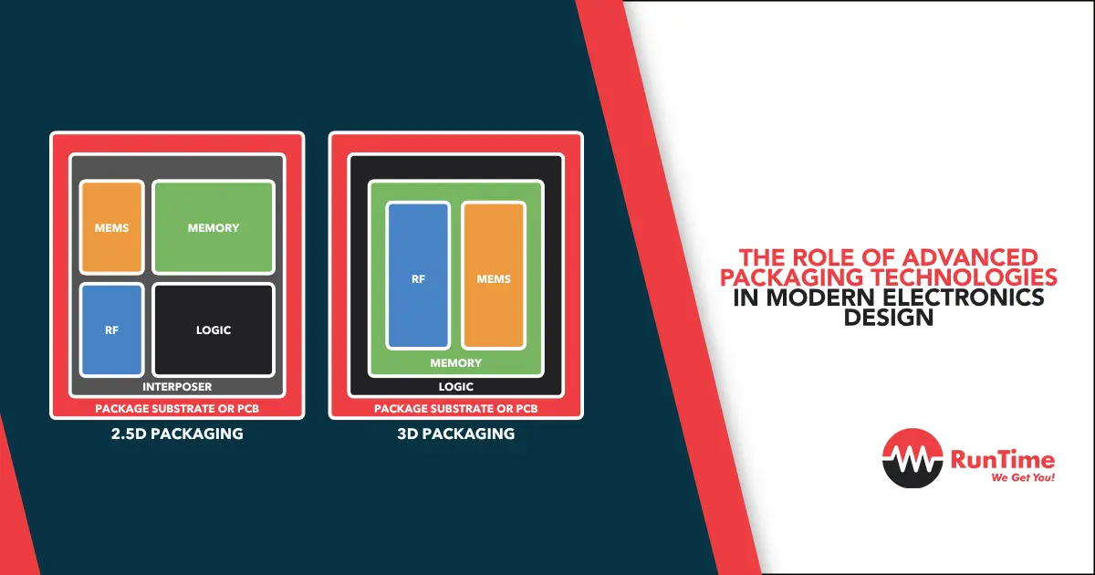
A. 2.5D and 3D Packaging
2.5D and 3D packaging involve stacking multiple chips vertically or placing them side-by-side on an interposer, a silicon or organic layer that provides electrical connections.
- 2.5D Packaging: Chips are placed side-by-side on an interposer, which connects them to the substrate. This is commonly used for high-bandwidth memory (HBM) integration.
- 3D Packaging: Chips are stacked vertically, allowing for shorter interconnects and higher density. This is ideal for applications requiring high performance and miniaturization.
B. Fan-Out Wafer-Level Packaging (FOWLP)
FOWLP is a packaging technology that allows chips to be placed directly on a substrate without the need for a traditional lead frame. This results in a smaller footprint and better electrical performance.
- Advantages:
- Reduced package size
- Improved thermal and electrical performance
- Lower cost compared to traditional packaging
- Applications: Mobile devices, automotive electronics, and IoT sensors.
C. System-in-Package (SiP)
SiP integrates multiple chips (e.g., processors, memory, RF modules) into a single package, enabling heterogeneous integration.
- Advantages:
- Reduced system size and weight
- Improved performance and power efficiency
- Simplified PCB design
- Applications: Wearables, smartphones, and medical devices.
D. Chiplet-Based Design
Chiplets are small, modular chips that can be combined to create a larger system. This approach allows for greater flexibility and scalability in design.
- Advantages:
- Reuse of proven IP blocks
- Reduced development time and cost
- Improved yield and manufacturability
- Applications: High-performance computing, AI accelerators, and data centers.
E. Embedded Die Packaging
In embedded die packaging, the chip is embedded directly into the substrate, eliminating the need for a separate package.
- Advantages:
- Ultra-compact form factor
- Improved thermal performance
- Enhanced reliability
- Applications: Automotive electronics, industrial sensors, and IoT devices.
4. Implications for Embedded Systems Design
Advanced packaging technologies are transforming the way embedded systems are designed. Here’s how:
A. Miniaturization
Advanced packaging enables smaller and lighter devices, which is critical for applications like wearables, IoT, and portable electronics.
B. Improved Performance
Shorter interconnects and higher integration density reduce latency and improve signal integrity, enhancing overall system performance.
C. Power Efficiency
Advanced packaging techniques like 3D stacking and FOWLP reduce power losses and improve thermal management, leading to more energy-efficient designs.
D. Heterogeneous Integration
Embedded engineers can now integrate diverse components (e.g., processors, memory, sensors) into a single package, simplifying system design and reducing time-to-market.
E. Cost Optimization
By enabling the reuse of chiplets and optimizing manufacturing processes, advanced packaging can reduce development and production costs.
5. Challenges in Advanced Packaging
While advanced packaging offers numerous benefits, it also presents several challenges:
- Thermal Management: Higher integration density can lead to increased heat generation, requiring innovative cooling solutions.
- Signal Integrity: Shorter interconnects and higher frequencies can introduce signal integrity issues like crosstalk and electromagnetic interference (EMI).
- Manufacturing Complexity: Advanced packaging techniques require sophisticated manufacturing processes and equipment.
- Testing and Validation: Ensuring the reliability and performance of complex packages is more challenging than traditional packaging.
- Cost: While advanced packaging can reduce costs in some cases, the initial investment in new technologies and processes can be high.
6. Best Practices for Leveraging Advanced Packaging
To successfully incorporate advanced packaging into embedded systems design, follow these best practices:
- Collaborate with Packaging Experts: Work closely with packaging engineers and manufacturers to optimize the design.
- Simulate and Model: Use simulation tools to analyze thermal, electrical, and mechanical performance.
- Focus on Thermal Management: Implement effective cooling solutions to manage heat dissipation.
- Design for Testability: Incorporate testability features to simplify validation and debugging.
- Stay Updated on Trends: Keep abreast of the latest advancements in packaging technologies and materials.
7. Case Studies: Advanced Packaging in Action
A. Apple’s M1 Chip
Apple’s M1 chip uses advanced packaging techniques like FOWLP and SiP to integrate CPU, GPU, memory, and other components into a single package, delivering exceptional performance and power efficiency.
B. AMD’s Chiplet-Based Processors
AMD’s Ryzen and EPYC processors leverage chiplet-based design to combine multiple CPU cores and I/O dies, enabling scalability and cost efficiency.
C. Tesla’s Full Self-Driving (FSD) Computer
Tesla’s FSD computer uses advanced packaging to integrate custom AI accelerators, memory, and other components, enabling real-time processing for autonomous driving.
8. Future Trends in Advanced Packaging
As the demand for smaller, faster, and more efficient devices continues to grow, advanced packaging technologies will play an increasingly important role. Here are some future trends to watch:
- Hybrid Bonding: A technique that enables direct bonding of chips without the need for solder bumps, further reducing interconnect lengths and improving performance.
- Glass Substrates: Glass offers superior electrical and thermal properties compared to traditional organic substrates, making it a promising material for future packaging.
- AI-Driven Design: Machine learning and AI will be used to optimize packaging designs for performance, power, and cost.
- Quantum Computing Packaging: Advanced packaging will be critical for enabling the complex interconnects and cooling requirements of quantum computers.
9. Tools and Resources for Advanced Packaging Design
Several tools and resources can help embedded engineers design with advanced packaging technologies:
A. Simulation Tools
- ANSYS: For thermal, electrical, and mechanical simulation.
- Cadence: Offers tools for signal integrity analysis and package design.
- Synopsys: Provides solutions for 3D-IC and advanced packaging design.
B. Industry Standards
- JEDEC Standards: Define guidelines for packaging and interconnect technologies.
- IEEE Standards: Provide frameworks for advanced packaging and heterogeneous integration.
C. Collaborative Platforms
- IMEC: A research organization focused on advanced semiconductor and packaging technologies.
- SEMI: An industry association that promotes collaboration and standardization in packaging.
Conclusion
Advanced packaging technologies are revolutionizing the way embedded systems are designed, enabling smaller, faster, and more efficient devices. For embedded engineers, understanding and leveraging these technologies is essential for staying competitive in a rapidly evolving industry.
By embracing advanced packaging techniques like 2.5D/3D packaging, FOWLP, and chiplet-based design, engineers can overcome the limitations of traditional packaging and unlock new possibilities in performance, power efficiency, and functionality. While challenges remain, the opportunities presented by advanced packaging are immense, paving the way for the next generation of embedded systems.
As the electronics industry continues to push the boundaries of innovation, advanced packaging will remain a cornerstone of modern electronics design. By staying informed and adopting best practices, embedded engineers can harness the full potential of these technologies to create groundbreaking products that shape the future.


