Field-Programmable Gate Arrays (FPGAs) are powerful tools for embedded engineers, offering the flexibility to implement custom hardware designs and accelerate complex algorithms. However, one of the most significant challenges in FPGA design is achieving timing closure—ensuring that all signals in the design meet their timing requirements. Timing closure is critical for the correct operation of the FPGA, as failing to meet timing constraints can lead to functional errors, reduced performance, or even complete system failure.
For embedded engineers, mastering the art of timing closure is essential for delivering reliable and high-performance FPGA designs. This article will explore the common timing closure challenges in FPGA projects, their root causes, and practical strategies to overcome them. By the end, you’ll have a comprehensive understanding of how to achieve timing closure and optimize your FPGA designs.
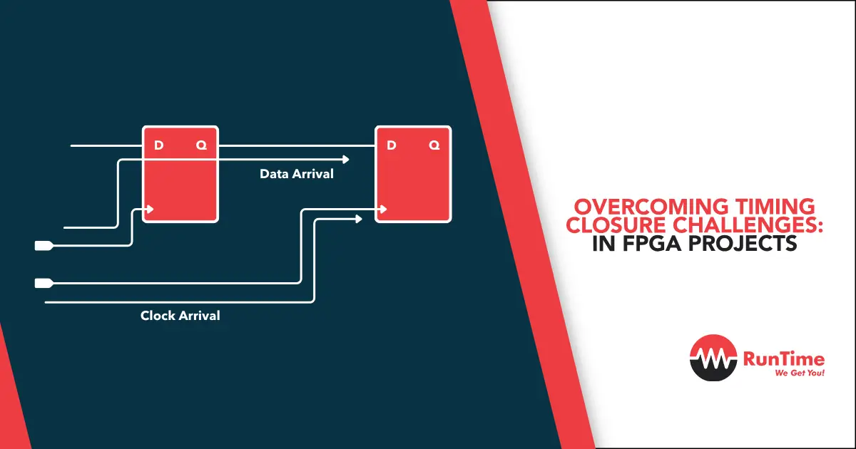
1. What is Timing Closure?
Timing closure is the process of ensuring that all signals in an FPGA design meet their required timing constraints. These constraints include:
- Setup Time: The time required for a signal to stabilize before the clock edge.
- Hold Time: The time required for a signal to remain stable after the clock edge.
- Clock-to-Q Delay: The time it takes for a signal to propagate from the clock input to the output of a flip-flop.
- Clock Skew: The difference in arrival times of the clock signal at different flip-flops.
Timing closure is achieved when the design meets all these constraints, ensuring reliable operation at the target clock frequency.
2. Why Timing Closure is Challenging
Timing closure is a complex and iterative process due to several factors:
- High Clock Frequencies: As clock frequencies increase, the margin for error decreases, making timing constraints harder to meet.
- Complex Designs: Large designs with many interconnected modules and high resource utilization can introduce timing bottlenecks.
- Routing Delays: The physical routing of signals on the FPGA fabric can introduce unpredictable delays.
- Clock Domain Crossings: Synchronizing signals between different clock domains adds complexity to timing analysis.
- Tool Limitations: FPGA synthesis and place-and-route tools may not always optimize timing effectively.
3. Common Timing Closure Challenges
Let’s explore the most common timing closure challenges and their root causes:
A. Long Combinational Paths
Long combinational paths between flip-flops can cause setup time violations. These paths often arise from complex logic or poor design partitioning.
B. High Fanout Nets
Signals with high fanout (driving many loads) can experience increased routing delays, leading to timing violations.
C. Clock Skew
Uneven clock distribution can cause clock skew, where the clock signal arrives at different flip-flops at different times.
D. Clock Domain Crossings
Transferring signals between clock domains without proper synchronization can lead to metastability and timing violations.
E. Resource Congestion
High resource utilization can lead to suboptimal placement and routing, increasing delays and making timing closure harder to achieve.
4. Strategies for Overcoming Timing Closure Challenges
Achieving timing closure requires a combination of good design practices, optimization techniques, and tool-specific strategies. Here are some practical approaches:
A. Design for Timing
- Pipeline Your Design: Break long combinational paths into smaller stages by adding pipeline registers.
- Limit Combinational Logic: Keep combinational logic between flip-flops as simple as possible.
- Use Synchronous Design Practices: Avoid asynchronous logic and ensure all signals are synchronized to a clock.
B. Optimize Clocking
- Use Global Clock Buffers: Ensure clocks are distributed evenly using global clock buffers.
- Minimize Clock Skew: Balance clock tree synthesis to reduce skew.
- Clock Gating: Use clock gating carefully to avoid introducing timing issues.
C. Reduce Fanout
- Replicate High-Fanout Signals: Duplicate drivers to reduce the load on high-fanout nets.
- Use Hierarchical Design: Partition the design into smaller modules to limit fanout.
D. Handle Clock Domain Crossings
- Use Synchronizers: Add synchronizers (e.g., two-flop synchronizers) for signals crossing clock domains.
- FIFO Buffers: Use FIFOs for transferring data between clock domains.
E. Optimize Placement and Routing
- Floorplanning: Manually place critical modules to reduce routing delays.
- Timing Constraints: Define accurate timing constraints to guide the tools.
- Incremental Compilation: Use incremental compilation to preserve timing-critical placements.
F. Leverage FPGA Tools
- Timing Analysis: Use static timing analysis (STA) tools to identify and resolve timing violations.
- Retiming: Allow the tools to move registers across combinational logic to balance delays.
- Multi-Pass Compilation: Run multiple compilation passes to explore different optimization strategies.
5. Best Practices for Timing Closure
To achieve timing closure efficiently, follow these best practices:
- Start Early: Consider timing constraints from the beginning of the design process.
- Use Hierarchical Design: Break the design into manageable modules with clear interfaces.
- Simulate and Verify: Use simulation to validate timing-critical paths before synthesis.
- Iterate and Optimize: Be prepared to iterate on the design and synthesis process to achieve timing closure.
- Collaborate with Experts: Work with experienced FPGA designers and tool vendors to address complex timing issues.
6. Tools and Techniques for Timing Closure
Several tools and techniques can help embedded engineers achieve timing closure:
A. Static Timing Analysis (STA)
STA tools analyze the design to identify timing violations and provide detailed reports.
- Xilinx Vivado: Includes powerful STA tools for Xilinx FPGAs.
- Intel Quartus: Offers timing analysis and optimization features for Intel FPGAs.
B. Floorplanning Tools
Floorplanning tools allow you to manually place critical modules to optimize timing.
- Xilinx PlanAhead: A floorplanning tool integrated with Vivado.
- Intel Chip Planner: Provides floorplanning capabilities in Quartus.
Timing Constraints
Defining accurate timing constraints is critical for guiding the synthesis and place-and-route tools.
- SDC (Synopsys Design Constraints): A standard format for timing constraints.
- XDC (Xilinx Design Constraints): Used in Xilinx tools.
Incremental Compilation
Incremental compilation preserves timing-critical placements and reduces compilation time.
- Xilinx Vivado: Supports incremental compilation for large designs.
- Intel Quartus: Offers incremental compilation features.
Case Studies: Timing Closure in Real-World Projects
A. High-Speed Data Acquisition System
A high-speed data acquisition system required precise timing to capture data at 1 GHz. By pipelining the design and optimizing clock distribution, the team achieved timing closure.
B. Video Processing Pipeline
A video processing pipeline faced timing violations due to long combinational paths. Using retiming and floorplanning, the designers resolved the issues and met the target clock frequency.
C. Wireless Communication System
A wireless communication system struggled with clock domain crossings. By adding synchronizers and FIFOs, the team ensured reliable operation across clock domains.
Future Trends in Timing Closure
As FPGA designs become more complex, new trends are emerging to address timing closure challenges:
- AI-Driven Optimization: Using machine learning to optimize placement and routing.
- High-Level Synthesis (HLS): Automating timing-aware design at a higher abstraction level.
- 3D FPGAs: Leveraging 3D stacking to reduce routing delays and improve timing.
Conclusion
Timing closure is a critical aspect of FPGA design that requires careful planning, optimization, and iteration. By understanding the common challenges and implementing best practices, embedded engineers can achieve timing closure and deliver high-performance FPGA designs.
Whether you’re working on high-speed data acquisition, video processing, or wireless communication, mastering the art of timing closure will enable you to create robust and reliable FPGA systems. As FPGA technology continues to evolve, staying ahead of the curve will require continuous learning and adaptation. Happy designing!


