FPGAs (Field-Programmable Gate Arrays) are highly regarded for their unparalleled flexibility in real-time processing. However, their full potential is realized when they are connected to external peripherals that enhance their capabilities. This article explores the complexities of connecting FPGAs to two widely used communication protocols – SPI (Serial Peripheral Interface) and I2C (Inter-Integrated Circuit) – from the perspective of the FPGA acting as the master device.
Technical Nuances: SPI vs I2C
The choice between SPI and I2C hinges on the specific application requirements. Here’s a technical breakdown to guide your decision:
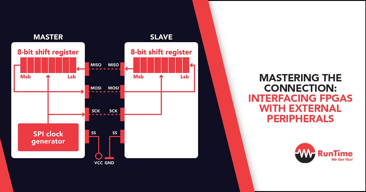
- SPI: A high-speed, full-duplex protocol ideal for scenarios demanding fast data exchange. It utilizes four dedicated lines: Serial Clock (SCK), Master Out Slave In (MOSI), Master In Slave Out (MISO), and Slave Select (SS). The master controls the SCK and initiates communication by asserting the appropriate SS line for the targeted slave device. Data is transmitted and received simultaneously on MOSI and MISO lines, enabling efficient bi-directional communication.
- FPGA Master Implementation: The FPGA master requires dedicated logic blocks to generate the SCK signal, manage data transmission on MOSI, receive data on MISO, and assert/de-assert the appropriate SS line based on the targeted slave device.
- Advanced Features: The FPGA’s programmability allows for advanced features like hardware flow control. By implementing transmit and receive FIFOs (First-In-First-Out) buffers, data flow between the FPGA and peripheral can be optimized. The master can stall data transmission when the slave’s receive buffer is full and resume when it becomes available. This prevents data loss and ensures smooth communication.
- I2C: A multi-master, multi-slave protocol designed for low-power and low-speed communication. It thrives in situations where numerous peripherals share the same bus. I2C only requires two lines, Serial Data Line (SDA) and Serial Clock Line (SCL). Both master and slave devices can initiate communication, with arbitration logic resolving any conflicts. Data is transferred serially, with each bit followed by an acknowledgement pulse to ensure transmission integrity.
- FPGA Master Implementation: The FPGA master needs logic to generate the SCL signal, drive data onto the SDA line, and sample data received on the SDA line. Additionally, logic for address generation, arbitration (if multiple masters are present), and acknowledgement generation is required.
Innovation Through Customization
The beauty of FPGAs lies in their programmability. For SPI, the master interface can be tailored to accommodate a wide range of clock frequencies and data sizes. Advanced features like hardware flow control can be implemented to optimize data exchange based on the specific peripheral’s characteristics.
For I2C, innovation can take the form of custom addressing schemes or the development of error detection and correction mechanisms to enhance communication robustness, particularly in noisy environments. Additionally, the FPGA’s inherent parallelism can be leveraged to manage multiple I2C slave devices concurrently, improving system efficiency. Here are some specific examples:
- Custom Addressing Schemes (I2C): The standard I2C addressing scheme allows for 128 unique devices. However, for systems with a larger number of peripherals, the FPGA master can be programmed to implement a custom multi-byte addressing scheme to expand the addressable space.
- Error Detection and Correction (I2C): While I2C includes a basic acknowledgement mechanism, the FPGA master can implement more sophisticated error detection and correction techniques like CRC (Cyclic Redundancy Check) to ensure data integrity in critical applications.
- Parallel I2C Transactions (I2C): By utilizing the FPGA’s parallel processing capabilities, the master interface can initiate communication with multiple slave devices simultaneously on the I2C bus. This can significantly improve data transfer rates for specific use cases where multiple peripherals require frequent data exchange with the FPGA.
Optimizing Performance
A critical aspect of FPGA-to-peripheral interfacing is achieving optimal performance. Here’s an analytical approach:
- Timing Analysis: Precise timing constraints are essential. For SPI, meticulous analysis of clock skew between SCK and data lines (MOSI and MISO) is crucial. Any significant skew can lead to data corruption. For I2C, ensuring proper rise and fall times on SDA and SCL lines is paramount to meet the protocol’s specified hold and set-up times. Timing analysis tools integrated within FPGA development environments are crucial for verifying timing closure.
- Resource Utilization: FPGA resources are finite. Analyzing the trade-off between implementing complex communication protocols
Conclusion
Interfacing FPGAs with external peripherals using SPI and I2C unlocks a world of possibilities in embedded system design. By understanding the technical nuances of each protocol, coupled with an innovative mindset and an analytical approach to performance optimization, field engineers can harness the true potential of FPGAs, propelling their projects to the forefront of technological advancement.
Hire the Best Engineers with RunTime
At RunTime, we are dedicated to helping you find the best Engineering talent for your recruitment needs. Our team consists of engineers-turned-recruiters with an extensive network and a focus on quality. By partnering with us, you will have access to great engineering talent that drives innovation and excellence in your projects.
Discover how RunTime has helped 423+ tech companies find highly qualified and talented engineers to enhance their team’s capabilities and achieve strategic goals.
On the other hand, if you’re a control systems engineer looking for new opportunities, RunTime Recruitment’s job site is the perfect place to find job vacancies.


