In the world of embedded engineering, high-frequency circuit design is becoming increasingly important as modern systems push for faster processing and higher bandwidth. As the operating frequency of circuits increases, parasitic effects become more pronounced, causing unintentional behavior that can degrade performance or lead to outright system failure. Understanding and mitigating parasitics is critical for ensuring the reliability of high-speed circuits.
In this article, we’ll delve into the nature of parasitic effects in high-frequency circuit design, examine the common sources of parasitics, and discuss best practices for minimizing these unwanted phenomena.
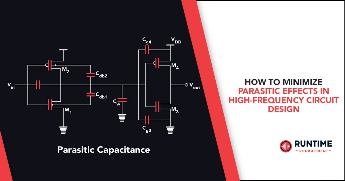
What Are Parasitic Effects?
Parasitics refer to unintended resistances, capacitances, and inductances present in electronic circuits. While these elements are usually negligible in low-frequency circuits, they become significant in high-frequency environments, where their impact can lead to signal loss, interference, and distortion. In high-frequency design, parasitic effects can:
- Alter impedance characteristics
- Degrade signal integrity
- Cause power loss
- Generate electromagnetic interference (EMI)
- Affect timing accuracy in digital circuits
Understanding the origins of parasitics and knowing how to control them is essential for effective high-frequency design.
Sources of Parasitic Effects
Parasitic elements arise from several aspects of circuit design, including:
- PCB Layout: The physical layout of printed circuit boards (PCBs) introduces parasitic inductance, capacitance, and resistance.
- Components: Every passive and active component (such as resistors, capacitors, transistors, and even connectors) has parasitic properties, even if they are not explicitly included in the component’s datasheet.
- Wiring and Traces: Conductive traces, wires, and vias all have associated parasitic resistance, capacitance, and inductance.
- Ground Planes: An improper ground plane design can create unwanted noise, signal reflections, and increased parasitic impedance.
- Interconnects: Connectors, cables, and solder joints introduce parasitics that can degrade signal transmission.
Let’s break down each source and discuss methods for minimizing parasitic effects.
1. PCB Layout: The Foundation of High-Frequency Design
At high frequencies, the PCB layout is as important as the circuit design itself. Poor layout decisions can lead to parasitics that undermine circuit performance. Here are several techniques to minimize parasitic effects in PCB design:
Shorten Trace Lengths
Longer traces introduce more parasitic inductance and resistance. To minimize these effects:
- Keep traces as short as possible, especially for high-speed signals and power delivery paths.
- Use direct routes with minimal bends and avoid meandering traces, as they increase inductance.
Use Controlled Impedance Traces
At high frequencies, signals require controlled impedance to avoid reflections and losses. Design traces with specific impedance characteristics (such as 50 ohms for RF signals):
- Use microstrip or stripline structures to control impedance, depending on the signal frequency and the layer stack-up.
- Calculate trace widths and spacing carefully to maintain the desired impedance. Tools like transmission line calculators are essential here.
Minimize Via Usage
Each via introduces parasitic inductance and capacitance. To reduce the number of vias:
- Route high-speed signals on the same layer whenever possible.
- If a via is necessary, keep its length short and avoid using multiple vias in series.
- For critical signals, consider using blind or buried vias to minimize their impact.
Ensure Proper Grounding
The ground plane plays a crucial role in minimizing parasitic inductance and resistance:
- Use a solid ground plane directly beneath signal traces to provide a low-inductance return path.
- Ensure continuous ground connections between different layers of the PCB.
- Avoid splitting the ground plane, as this can cause signal reflection and create high-impedance return paths.
Separate Power and Signal Traces
Power and signal traces should be kept separate to reduce coupling and noise:
- Route power and ground planes on dedicated layers to minimize parasitic capacitance.
- For sensitive signals, use ground shielding (i.e., ground traces or planes placed close to the signal traces) to minimize crosstalk.
2. Components: Accounting for Parasitic Properties
Every component in a high-frequency circuit has inherent parasitic inductance, capacitance, and resistance, which must be considered in the design process.
Capacitors and Inductors
Parasitic inductance in capacitors and parasitic capacitance in inductors can alter their behavior at high frequencies:
- Use high-frequency capacitors (e.g., ceramic capacitors) with low equivalent series inductance (ESL) for decoupling applications.
- Choose inductors with low equivalent series resistance (ESR) and self-resonant frequencies (SRF) above the operating frequency of your circuit.
- Always check the parasitic characteristics of components in their datasheets and simulate them in circuit simulations.
Resistors
Resistors exhibit parasitic inductance at high frequencies, which can distort signal integrity:
- Use surface-mount resistors (SMT) instead of through-hole resistors to reduce parasitic inductance.
- Choose low-inductance resistors designed for high-frequency applications.
Active Components
Transistors, diodes, and integrated circuits (ICs) also have parasitic elements that can affect high-frequency performance:
- Choose components with low package inductance and capacitance.
- For high-speed transistors, ensure that their transition frequency (ft) is well above the operating frequency of your circuit.
- Place decoupling capacitors close to the power pins of ICs to reduce parasitic inductance and improve power integrity.
3. Wiring and Traces: Reducing Parasitic Effects in Connections
The connections between components, including PCB traces, vias, and connectors, introduce parasitics that must be managed carefully.
Minimize Parasitic Inductance
Inductance arises from loops in the current path, and minimizing loop area reduces inductance:
- Use short, wide traces for power and ground connections.
- Minimize loop areas by routing signal and return paths close to each other (for example, by placing signal traces over a solid ground plane).
Reduce Parasitic Capacitance
The capacitance between adjacent traces can cause signal coupling, leading to crosstalk:
- Keep signal traces adequately spaced to reduce parasitic capacitance.
- Use ground shielding between high-speed signal traces to reduce crosstalk.
Twisted Pair and Differential Signaling
For long signal paths, such as those found in differential signaling (e.g., LVDS), consider using twisted-pair cabling or controlled-impedance differential pairs on the PCB:
- Twisted pair cables cancel out parasitic inductance and capacitance by ensuring that the fields generated by each wire cancel each other out.
- On PCBs, use matched differential pairs with consistent trace width and spacing to ensure minimal signal distortion and reduce the impact of parasitics.
4. Ground Planes: Mitigating Ground Loop and Impedance Issues
The ground plane serves as the return path for many high-frequency signals, and improper grounding can cause parasitic effects such as ground loops, increased noise, and EMI.
Use a Single Ground Plane
In high-frequency design, it’s crucial to maintain a low-impedance ground path:
- Use a single, continuous ground plane in multilayer PCBs to provide a solid return path for all signals.
- Avoid splitting the ground plane into multiple isolated sections, as this can create high-impedance return paths and lead to ground loops.
Shorten Ground Loops
Ground loops introduce parasitic inductance and EMI issues:
- Ensure that signal and ground traces follow the same route and are kept close together to reduce the loop area.
- For high-speed signals, use a dedicated ground plane as a reference to minimize the risk of forming ground loops.
Implement Ground Shields
Ground shielding can reduce EMI and parasitic coupling:
- Place ground traces or planes between signal traces to shield them from parasitic capacitance.
- For critical signal traces, use stitching to connect the top and bottom ground planes, further reducing loop inductance.
5. Interconnects: Minimizing Parasitic Effects in Connectors and Cables
Connectors, cables, and solder joints introduce parasitics that can distort high-frequency signals.
Choose High-Frequency Connectors
Select connectors specifically designed for high-frequency applications:
- Use connectors with minimal inductance and capacitance, such as those with short pin lengths and well-shielded structures.
- For RF and microwave circuits, use coaxial connectors (e.g., SMA connectors) to maintain impedance matching and reduce parasitics.
Minimize Parasitic Capacitance in Solder Joints
Solder joints can introduce unwanted parasitic capacitance:
- Ensure clean, minimal solder joints by using the right amount of solder paste during assembly.
- Avoid cold solder joints, which can create excess parasitic effects due to increased contact resistance and inductance.
Optimize Cable Lengths
For signal cables, especially at high frequencies:
- Keep cable lengths as short as possible to minimize parasitic inductance and capacitance.
- Use shielded cables to reduce noise pickup and parasitic coupling between signal lines.
Simulation and Prototyping: The Importance of Validation
Even with careful design, parasitic effects can still surprise you during prototyping. Therefore, it’s important to validate your design using:
High-Frequency Simulation Tools
Use simulation software (such as SPICE or EM simulators) to model parasitic elements in your circuit:
- Include parasitic inductance, capacitance, and resistance in your models.
- Perform signal integrity and power integrity analyses to identify potential issues before moving to prototyping.
Prototyping and Testing
After simulation, build and test prototypes to measure real-world parasitics:
- Use vector network analyzers (VNAs) and oscilloscopes to measure signal integrity and detect parasitic-induced performance degradation.
- Test for EMI, crosstalk, and signal distortion in the final design, iterating as needed to reduce parasitics.
Conclusion: Parasitics are Inevitable but Controllable
Parasitic effects are unavoidable in high-frequency circuit design, but with proper planning, layout, and component selection, their impact can be minimized. The key to success lies in understanding where parasitics come from and taking steps to mitigate them through careful design choices, simulation, and validation.
By following the best practices outlined here, you can reduce parasitic inductance, capacitance, and resistance, ensuring your high-frequency circuits perform reliably and meet your design goals.


