In the realm of high-speed digital circuits, minimizing ground bounce is paramount to ensure signal integrity and prevent malfunctions. Ground bounce, a phenomenon where the ground voltage fluctuates due to rapid signal transitions, can lead to timing errors and signal degradation. This issue becomes more critical as circuit speeds increase, making effective mitigation strategies essential. By understanding the root causes of ground bounce, such as simultaneous switching noise and parasitic inductance, engineers can implement various techniques to curb its effects.
Techniques like proper decoupling, controlled impedance routing, and careful component placement play a vital role in reducing ground bounce. This comprehensive guide will delve into the intricacies of ground bounce in high-speed digital circuits and provide practical insights on how to minimize its impact, ensuring robust circuit performance and reliable operation in demanding applications.
Root Causes of Ground Bounce
Ground bounce is a prevalent issue in digital circuits, especially in high-speed designs. It occurs when there are sudden voltage fluctuations in the ground connections due to rapid current changes during signal transitions. To ensure the reliability and functionality of electronic systems, it is crucial to understand the primary causes of ground bounce and implement effective solutions.
Impact of Switching Characteristics on Ground Bounce
The switching characteristics of digital components significantly contribute to ground bounce. When signals change states, abrupt current spikes can occur, causing disruptions in the ground plane’s voltage levels. Analyzing and optimizing the switching behavior of components is essential to minimize ground bounce effects and maintain signal integrity.
Influence of PCB Layout on Ground Bounce
The layout of the printed circuit board (PCB) plays a pivotal role in managing ground bounce. Factors such as improper routing, inadequate ground plane design, and lack of decoupling capacitors can worsen ground bounce issues. Designers must focus on optimizing the PCB layout, employing proper grounding techniques, and ensuring signal paths are optimized to reduce ground bounce.
Addressing Signal Integrity Challenges to Combat Ground Bounce
Maintaining signal integrity is paramount in addressing ground bounce-related problems. Strategies like managing signal reflections, reducing crosstalk, and controlling impedance mismatches are vital for minimizing ground bounce effects. Designers should adhere to signal integrity best practices, including impedance matching, transmission line design considerations, and proper termination methods to enhance circuit reliability.
Additional Considerations for Ground Bounce Mitigation
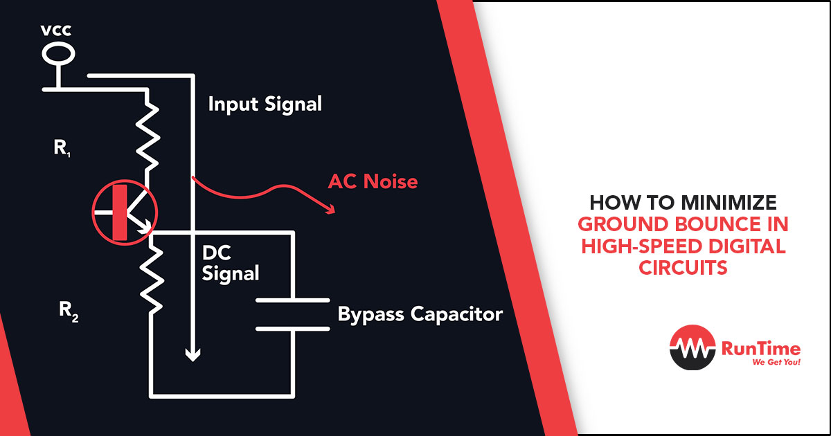
Apart from the primary factors contributing to ground bounce, several other considerations can help in effectively mitigating this issue. One crucial aspect is the use of bypass capacitors strategically placed near integrated circuits to stabilize the power distribution network and reduce voltage fluctuations during switching events.
Moreover, implementing controlled impedance traces for high-speed signal paths can minimize signal distortions and reduce reflections that could exacerbate ground bounce. Ensuring a balanced stackup in multilayer PCB designs, with careful attention to signal and ground plane allocations, can also aid in reducing ground bounce effects.
Furthermore, utilizing simulation tools and conducting thorough signal integrity analyses during the design phase can provide valuable insights into potential ground bounce areas and enable preemptive measures to be taken. By simulating signal behavior under various scenarios and optimizing the layout based on simulation results, designers can proactively address ground bounce challenges and refine their designs for improved performance.
A comprehensive understanding of the root causes of ground bounce and meticulous attention to mitigating strategies are imperative for achieving robust and stable performance in digital electronic systems. By incorporating advanced design techniques, leveraging simulation tools, and following industry best practices, designers can effectively combat ground bounce issues and elevate the overall quality and reliability of their electronic designs.
Negative Impacts of Ground Bounce
Deterioration of Signal Integrity
Ground bounce can result in the deterioration of signal integrity in electronic circuits. When ground bounce occurs, it can introduce noise and interference to the signals being transmitted, leading to potential errors or malfunctions in the system.
Timing Discrepancies
Another significant impact of ground bounce is the introduction of timing discrepancies in the circuit. The bouncing of the ground can cause variations in signal propagation times, affecting the synchronization of different components within the system. This can lead to timing issues and ultimately impact the overall performance of the circuit.
Risk of Component Damage
Ground bounce poses a risk of causing damage to electronic components within the circuit. The rapid fluctuations in voltage levels resulting from ground bounce can exceed the maximum ratings of components, leading to overvoltage stress and potential failures. This risk highlights the importance of addressing and mitigating ground bounce in electronic designs.
Electrical Noise
In addition to signal integrity issues, ground bounce can also contribute to increased electrical noise within electronic circuits. The bouncing ground can create unwanted noise that interferes with the normal operation of the system, potentially affecting the accuracy of data transmission and reception.
EMI and EMC Concerns
Ground bounce not only affects the internal operation of a circuit but also raises concerns related to Electromagnetic Interference (EMI) and Electromagnetic Compatibility (EMC). The unintended emissions resulting from ground bounce can lead to electromagnetic interference, causing disruptions in nearby electronic devices and systems. Ensuring proper grounding and layout practices is crucial to minimize EMI/EMC issues.
System Reliability
The cumulative effects of ground bounce on signal integrity, timing, component health, and noise levels ultimately impact the overall reliability of electronic systems. Unaddressed ground bounce issues can compromise the long-term performance and stability of electronic devices, emphasizing the need for thorough analysis and mitigation strategies.
Mitigation Techniques
To combat the negative impacts of ground bounce, engineers employ various mitigation techniques such as proper grounding schemes, decoupling capacitors, controlled impedance traces, and signal integrity analysis tools. By implementing these strategies during the design phase, it is possible to minimize the adverse effects of ground bounce and enhance the robustness of electronic circuits.
Effective Strategies to Reduce Ground Bounce
Ground bounce is a common issue in electronic circuits that can lead to signal integrity problems and performance issues. To address this challenge, it is essential to implement effective strategies to minimize ground bounce. In this blog section, we will explore key techniques to reduce ground bounce and improve overall circuit performance.
Optimization of Power Delivery Networks
Proper optimization of power delivery networks is crucial to reducing ground bounce. By ensuring a low impedance path for current flow and minimizing voltage fluctuations, the impact of ground bounce can be significantly reduced. Techniques such as using low-ESR capacitors, optimizing trace routing, and minimizing loop inductance can help improve power integrity and reduce ground bounce.
Strategic Placement of Decoupling Capacitors
Decoupling capacitors play a vital role in reducing ground bounce by providing a local charge reservoir to compensate for transient current demands. Strategic placement of decoupling capacitors near high-speed ICs and other critical components can help to suppress voltage fluctuations and minimize ground bounce effects. Proper selection of capacitor values and types based on the frequency of operation is also important to achieve optimal performance.
Utilizing Ground Plane Design Best Practices
Ground plane design is a key aspect of reducing ground bounce in PCB layouts. By following best practices such as creating solid ground planes, minimizing ground loops, and providing a low-impedance return path for currents, the effects of ground bounce can be mitigated. Careful consideration of layer stackup, signal return paths, and component placement can help optimize ground plane design and improve signal integrity.
Implementing Termination Techniques
Proper termination techniques are essential for reducing signal reflections and minimizing ground bounce in high-speed digital circuits. Techniques such as series terminations, parallel terminations, and source termination can help match impedance levels, control signal reflections, and reduce the effects of ground bounce. Selecting the appropriate termination scheme based on the signal characteristics and transmission line properties is critical for achieving reliable signal integrity and reducing ground bounce.
By implementing these effective strategies to reduce ground bounce, designers can improve the performance and reliability of electronic circuits. Addressing ground bounce issues early in the design process and following best practices for power delivery, decoupling, ground plane design, and termination can lead to better signal integrity and overall circuit operation.
Stay tuned for more insights on overcoming common challenges in electronic design and optimizing circuit performance!.
Importance of Simulation and Testing
Utilizing Simulation Tools for Ground Bounce Analysis
In the realm of electronic design and development, the importance of simulation and testing cannot be understated. These processes play a critical role in ensuring the reliability, efficiency, and performance of electronic systems. One key aspect where simulation and testing are crucial is in the analysis and minimization of ground bounce.
Ground bounce is a common phenomenon in electronic circuits where the ground voltage fluctuates due to rapid current changes. This can lead to various issues such as signal integrity problems, timing errors, and even device malfunction. To address these challenges, utilizing simulation tools for ground bounce analysis is essential.
Simulation tools, such as SPICE (Simulation Program with Integrated Circuit Emphasis), allow engineers to model and simulate the behavior of electronic circuits under different conditions. By simulating ground bounce effects, engineers can gain valuable insights into the causes of ground bounce and its impact on circuit performance.
Moreover, testing approaches play a vital role in validating the effectiveness of ground bounce minimization techniques. Through rigorous testing procedures, engineers can verify the functionality and reliability of the circuit in real-world scenarios. This process helps in identifying potential issues early on and implementing necessary design modifications to mitigate ground bounce effects.
In addition to SPICE, other simulation tools like LTspice and MATLAB/Simulink are commonly used in the industry for comprehensive circuit analysis and optimization. These tools enable engineers to not only simulate ground bounce but also assess other critical parameters such as noise immunity, power consumption, and thermal behavior.
Furthermore, advancements in simulation technology, such as the integration of artificial intelligence and machine learning algorithms, have revolutionized the way electronic systems are designed and tested. AI-driven simulations can predict potential ground bounce scenarios with greater accuracy, allowing engineers to proactively address issues before physical prototyping.
When it comes to testing, methodologies like boundary scan testing and in-circuit testing are instrumental in validating the functionality of complex PCB layouts and integrated circuits. These testing approaches help in detecting and rectifying ground bounce-related anomalies early in the design cycle, saving time and resources.
The combination of simulation tools and testing approaches is indispensable for addressing ground bounce challenges in electronic design. By leveraging these tools effectively, engineers can enhance the quality, reliability, and performance of electronic systems, ultimately leading to successful product development and deployment. The continuous evolution of simulation and testing methodologies underscores their significance in ensuring the robustness and competitiveness of modern electronic products.
Real-World Applications
Case Studies on Ground Bounce Mitigation
In this section, we will delve into real-world case studies that highlight the critical importance of ground bounce mitigation in electronic design. By examining these case studies, we can deepen our understanding of the challenges faced by engineers and the innovative strategies employed to tackle ground bounce issues effectively.
Industry Best Practices for Ground Bounce Mitigation
Moreover, we will explore industry best practices that play a pivotal role in mitigating ground bounce. By analyzing how leading companies approach this challenge, we can glean valuable insights and leverage proven methodologies in our own design projects to enhance overall system performance and reliability.
Real-World Applications of Ground Bounce Mitigation
Ground bounce is a prevalent issue in high-speed digital circuits that can significantly impact signal integrity and overall system functionality. Through real-world case studies spanning industries such as telecommunications, automotive, and consumer electronics, we will uncover the diverse manifestations of ground bounce and its implications on product reliability. By gaining insights into these practical scenarios, engineers can proactively implement measures to mitigate ground bounce effects and fortify the robustness of their designs.
Implementing Effective Strategies for Ground Bounce Mitigation
Beyond exploring case studies, it is imperative to identify and implement effective strategies for mitigating ground bounce in electronic systems. Industry best practices encompass a spectrum of techniques, including meticulous power distribution design, thorough signal integrity analysis, and strategic utilization of decoupling capacitors. By delving into these best practices and elucidating their real-world applications, engineers can elevate their design proficiencies and diminish the occurrence of ground bounce-related challenges in their projects. Join us on this enlightening journey as we unravel the intricacies of ground bounce mitigation and its pivotal role in ensuring the reliability and optimal performance of electronic systems.
Future Trends in Ground Bounce Management
Ground bounce is a common issue in high-speed digital circuits that can lead to malfunctions and performance degradation. As technology advances, new trends are emerging in ground bounce management to address these challenges. In this blog section, we will explore the latest advancements in circuit design and testing methodologies aimed at reducing ground bounce.
Advancements in Circuit Design for Ground Bounce Reduction
One of the key areas of focus in ground bounce management is circuit design. Engineers are continuously developing new techniques and strategies to minimize ground bounce in digital circuits. This includes the use of low-inductance power distribution networks, optimized signal routing, and innovative grounding schemes. By employing these design practices, engineers can effectively reduce the impact of ground bounce on circuit performance.
Innovations in Testing Methodologies
In addition to circuit design improvements, testing methodologies play a crucial role in identifying and mitigating ground bounce issues. Advanced simulation tools and test equipment allow engineers to accurately analyze the behavior of digital circuits under different operating conditions. By simulating ground bounce effects and conducting comprehensive testing, engineers can proactively address potential issues before they impact the final product.
Emerging Technologies for Ground Bounce Management
Beyond traditional approaches, emerging technologies are shaping the future of ground bounce management. Techniques such as adaptive impedance control, advanced noise filtering algorithms, and intelligent signal integrity analysis are gaining traction in the industry. These technologies offer enhanced precision and efficiency in mitigating ground bounce effects, paving the way for more reliable high-speed digital systems.
Role of Machine Learning in Ground Bounce Mitigation
Machine learning algorithms are increasingly being leveraged to optimize ground bounce mitigation strategies. By analyzing vast amounts of data and identifying complex patterns, machine learning models can predict and prevent potential ground bounce issues with high accuracy. This data-driven approach not only enhances the effectiveness of ground bounce management but also contributes to the overall efficiency and performance of digital circuits.
Conclusion
The future of ground bounce management is evolving rapidly with advancements in circuit design, testing methodologies, emerging technologies, and the integration of machine learning. By embracing these trends and innovations, engineers can overcome the challenges posed by ground bounce and ensure the reliability and performance of high-speed digital circuits in the dynamic landscape of electronics design and development.
Conclusion
Minimizing ground bounce in high-speed digital circuits is crucial to ensure reliable and robust circuit operation. By implementing proper design techniques such as optimizing return paths, using decoupling capacitors, and minimizing loop inductance, designers can effectively mitigate ground bounce issues. By understanding the causes and effects of ground bounce and taking proactive steps during the design phase, engineers can enhance the overall performance and signal integrity of their high-speed digital circuits.


