Block RAM (BRAM) is a cornerstone of FPGA design, offering high-speed, on-chip memory solutions crucial for efficient data handling. This article delves into the practical aspects of integrating BRAM into your FPGA design, providing a technical deep dive for those well-versed in the intricacies of hardware design. We’ll explore the nuances of BRAM architecture, optimization techniques, and real-world application considerations, ensuring you can make the most of this powerful resource.
Understanding BRAM Architecture
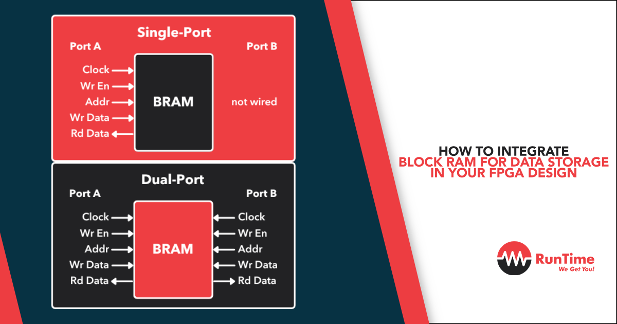
Before diving into integration, it’s essential to grasp the fundamental structure of BRAM. BRAM is a dual-port memory block capable of simultaneous reads and writes on independent ports. This dual-port nature is instrumental in pipelined architectures, enabling high throughput.
Port Configuration
BRAMs offer flexible port configurations, allowing you to tailor the memory to your specific needs. Consider factors like:
- Read/Write Enable: Controls when read or write operations are allowed.
- Clock Domains: Ensures data is synchronized properly across different parts of your design.
- Output Registers: Determines if the data is registered before being output, affecting timing and performance.
Depth and Width
The depth and width of a BRAM determine its capacity. Consider the following:
- Data Size: Match the BRAM size to your application’s data size to avoid wasted space.
- Access Patterns: Optimize memory layout based on how data is accessed and modified.
Single-Port vs. Dual-Port Mode
While dual-port mode offers higher throughput, it might introduce complexities in design and timing closure. Evaluate the trade-offs based on:
- Bandwidth Requirements: Dual-port can double the bandwidth for read and write operations.
- Design Complexity: Dual-port mode may complicate timing and routing, making it harder to meet design constraints.
Integrating BRAM into Your Design
Identify Memory Requirements
Analyze data flow and access patterns to determine the necessary memory size, access latency, and throughput. Consider:
- Data Types: (signed/unsigned, fixed-point/floating-point) and their corresponding bit widths.
- Memory Structures: FIFO or synchronous memory structures depending on your data flow requirements.
BRAM Instantiation
Utilize the appropriate HDL constructs (e.g., generate statement, memory primitives) to instantiate BRAMs. Pay attention to:
- Port Widths and Depths: Configure according to your design specifications.
- Clock Domains: Manage asynchronous interfaces if applicable.
Address and Data Path Design
Develop efficient address generation logic to access data within the BRAM. Key considerations include:
- Address Generation: Efficient logic to access different memory locations.
- Data Paths: Reading and writing data paths to/from the BRAM.
- Optimization: Data path width and register stages for performance and resource utilization.
Timing Constraints and Optimization
Apply careful timing constraints to ensure data integrity and meet performance goals. Techniques include:
- Timing Constraints: Ensure signals meet setup and hold times.
- BRAM Placement: Optimize placement and routing for critical paths.
- Vendor-Specific Optimization: Techniques like pipelining and clock gating.
Advanced BRAM Utilization Techniques
Distributed RAM vs. BRAM
Understand the trade-offs between distributed RAM and BRAM in terms of:
- Performance: BRAM generally offers higher performance for larger memory blocks.
- Capacity: BRAM provides larger, denser memory than distributed RAM.
- Resource Utilization: Distributed RAM can be more flexible for smaller, distributed memory needs.
BRAM-Based FIFOs
Design efficient FIFOs using BRAMs for high-speed data buffering and flow control. Considerations include:
- Data Buffering: Efficient storage and retrieval of data streams.
- Flow Control: Managing data flow to ensure smooth operation.
Memory Interleaving
Improve data access parallelism by interleaving data across multiple BRAMs. Benefits include:
- Parallelism: Enhanced throughput and efficiency of memory operations.
- Access Speed: Faster data retrieval by spreading access across multiple BRAMs.
BRAM-Based Lookup Tables
Utilize BRAMs for implementing large lookup tables for functions or data mapping. Advantages include:
- Function Mapping: Accelerate complex functions with precomputed results.
- Data Transformation: Quick data lookups for transformation tasks.
Case Studies and Real-World Applications
Image and Video Processing
BRAMs excel in storing and processing image and video frames, enabling real-time algorithms such as:
- Video Encoding/Decoding: Fast access to frame data for compression and decompression.
- Image Filtering: Real-time image enhancements and transformations.
- Object Detection: Rapid processing of image data for recognizing objects.
Digital Signal Processing (DSP)
BRAMs are crucial for storing coefficients, intermediate results, and FFT data in DSP systems. Applications include:
- Communications: High-performance signal modulation and demodulation.
- Audio Processing: Real-time audio filtering and enhancement.
- Sensor Data Analysis: Processing data from various sensors in real time.
Data Communication
BRAMs can be used for packet buffering, error correction coding, and protocol processing. Use cases include:
- Packet Buffering: Temporary storage of data packets during transmission.
- Error Correction: Storing codes for correcting transmission errors.
- Protocol Handling: Managing data according to communication protocols.
Machine Learning
BRAMs play a vital role in storing weights, activations, and intermediate results in neural networks. Key roles include:
- Weight Storage: Holding neural network weights for rapid access during inference.
- Activation Storage: Storing intermediate activations between layers.
- Intermediate Results: Efficient handling of temporary data during processing.
Conclusion
Effective BRAM integration is pivotal for optimizing FPGA designs. By understanding BRAM architecture, carefully considering memory requirements, and employing advanced techniques, designers can harness the full potential of on-chip memory for efficient data handling. Continuous exploration of new use cases and optimization methodologies will further advance the role of BRAMs in FPGA-based systems.
Integrating BRAM into your FPGA design is not just about adding memory; it’s about enhancing the overall system performance and capability. With careful planning and execution, BRAM can significantly elevate your FPGA projects, making them more robust and versatile. Whether you’re working on high-speed data processing, real-time video applications, or cutting-edge machine learning algorithms, BRAM offers the memory solutions you need to succeed.


