In the world of embedded systems, printed circuit board (PCB) design is a critical aspect of ensuring the reliable operation of devices, especially when dealing with mixed-signal systems. Mixed-signal PCBs combine both analog and digital circuits, which are inherently different in nature and often require careful planning to prevent noise, signal interference, and other issues that could compromise performance. Grounding is one of the most vital techniques to consider when designing mixed-signal PCBs. This article will explore effective grounding techniques and practices to mitigate noise and ensure optimal performance in mixed-signal systems.
Understanding Grounding in Mixed-Signal Systems
Before delving into specific techniques, it’s essential to understand the role of grounding in mixed-signal designs. Grounding provides a common reference point for all voltages in the system and helps to safely dissipate unwanted noise or interference. However, in mixed-signal designs, the interaction between analog and digital circuits can introduce challenges. Analog circuits are sensitive to noise, whereas digital circuits generate high-frequency switching noise. If not properly handled, the noise generated by the digital components can interfere with the analog circuitry, leading to performance degradation or even system failure.
The Primary Challenge: Noise Coupling
The crux of grounding challenges in mixed-signal designs lies in noise coupling. In these designs, digital components such as microcontrollers, FPGAs, and other ICs switch rapidly, causing ground currents that generate electromagnetic interference (EMI) and crosstalk. These unwanted signals can couple into sensitive analog components like amplifiers or ADCs (Analog-to-Digital Converters), affecting the accuracy and integrity of the signals they process. This makes effective grounding crucial to separating and mitigating these effects.
Common Grounding Approaches in Mixed-Signal Designs
To address noise coupling and other grounding-related issues, several techniques have been developed. These approaches vary based on the complexity and layout of the PCB, as well as the specific components involved. Here are some commonly used grounding techniques:
1. Single Ground Plane
One of the simplest approaches is to use a single ground plane for the entire PCB. The advantage of this method is that it reduces impedance by providing a large, low-resistance path for return currents. When properly designed, a single ground plane can effectively minimize voltage differences across the board, reducing noise coupling.
However, the downside of this approach is that it may allow digital noise to interfere with analog signals. Without careful separation of digital and analog components, digital noise currents can flow through the ground plane, disrupting sensitive analog circuits. Therefore, when using a single ground plane, component placement becomes critical.
Best Practices for Single Ground Planes:
- Careful Placement of Components: Digital and analog components should be placed in separate areas of the PCB. The digital circuits should be positioned closer to the power supply, while the analog circuits should be placed farther away to minimize noise interference.
- Minimize Current Loops: Keep the return paths for digital and analog signals as short as possible. This reduces the likelihood of interference from one circuit to another.
- Proper Decoupling: Use decoupling capacitors near the power pins of digital components to filter high-frequency noise. This can help prevent noise from spreading through the ground plane.
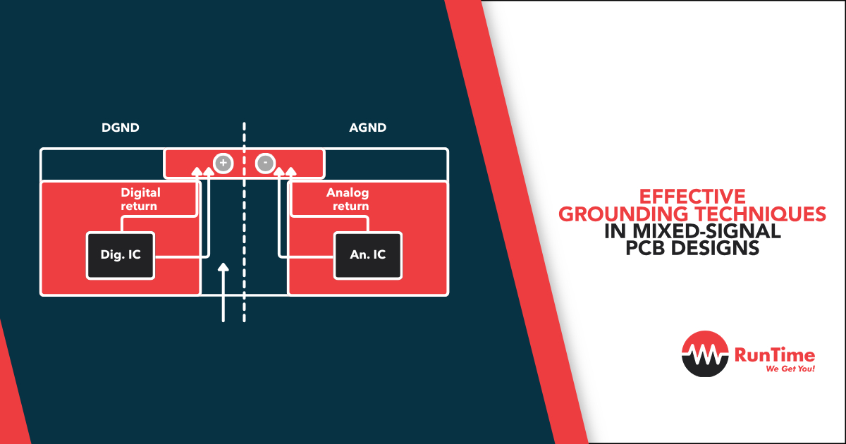
2. Split Ground Plane
Another common approach is to use a split ground plane, where the analog and digital sections of the PCB are separated by a physical gap in the ground plane. The analog and digital grounds are isolated, connected at only one point, usually near the power supply or a common reference point such as the ADC. This technique helps to prevent high-frequency noise generated by digital components from coupling into the analog circuits.
While a split ground plane offers better noise isolation, it requires careful design to avoid introducing other problems, such as ground loops or improper return paths.
Best Practices for Split Ground Planes:
- One Ground Connection: Ensure that the analog and digital ground planes are connected at a single point. Multiple ground connections can create ground loops, which will reintroduce noise into the system.
- Avoid Crossing Signals Over Gaps: Signals should not cross the gap between the analog and digital ground planes. Crossing signals over a split can introduce parasitic capacitance, which can lead to noise coupling.
- Ensure a Low-Impedance Path: The connection point between the analog and digital grounds should provide a low-impedance path for return currents. This is often done by placing the connection near a power supply or bypass capacitor.
3. Star Grounding
Star grounding is a technique where all ground connections are routed to a central point, like the spokes of a wheel. This method is especially useful in systems where multiple ground planes or grounding zones are needed. In a star grounding system, each section of the PCB has its own dedicated ground path, reducing the potential for noise to travel from one section to another.
Star grounding is particularly effective in high-precision analog circuits, where even the smallest amount of noise can affect performance. However, it is more complex to implement than a single or split ground plane, as it requires additional routing considerations.
Best Practices for Star Grounding:
- Use a Central Grounding Point: All ground connections should meet at a single, central location. This prevents the formation of ground loops, which can introduce noise.
- Isolate Critical Components: Components that are especially sensitive to noise, such as precision amplifiers or ADCs, should have their own dedicated ground paths that lead to the central grounding point.
- Minimize Ground Impedance: Ensure that all ground traces are as short and wide as possible to minimize impedance and allow for proper current flow.
4. Ground Fill or Copper Pour
Ground fills, also known as copper pours, are large areas of the PCB that are filled with copper and connected to the ground plane. These copper-filled areas help to reduce EMI by providing additional shielding and lowering the impedance of the ground plane. In mixed-signal designs, ground fills can be used to separate analog and digital sections or provide extra noise suppression for critical components.
Ground fills should be implemented carefully, as poor design choices can lead to unwanted parasitic effects or impedance issues.
Best Practices for Ground Fills:
- Ensure Proper Grounding: All copper fills should be connected to the ground plane with vias to ensure that they are properly grounded. Isolated ground fills can act as antennas, making the noise problem worse.
- Avoid Large Voids: Large voids in the ground fill can increase impedance and cause noise issues. Make sure that the copper pour is continuous and well-connected across the board.
- Use Multiple Vias: For larger PCBs, use multiple vias to connect the ground fill to the ground plane. This ensures that the entire board is properly grounded and reduces the likelihood of noise issues.
Component Placement and Signal Routing
In addition to choosing the right grounding technique, careful component placement and signal routing are crucial to the success of a mixed-signal design. Grounding issues often arise due to poor layout decisions, so attention to detail during the PCB layout phase is essential.
1. Separate Analog and Digital Components
One of the most important rules in mixed-signal PCB design is to keep analog and digital components separate. Placing them too close together can lead to noise coupling and signal degradation. Ideally, analog and digital components should have their own dedicated sections of the board, with separate power and ground planes or areas.
2. Route Signals Appropriately
When routing signals, it’s important to avoid crossing analog and digital signal traces. Crossing signals can introduce parasitic capacitance, leading to signal interference. Additionally, ensure that sensitive analog signals are routed away from high-speed digital signals to reduce the likelihood of noise coupling.
3. Minimize Crosstalk
Crosstalk occurs when the electromagnetic field from one signal trace interferes with another signal trace. To minimize crosstalk, keep signal traces as short and direct as possible. Use shielding techniques, such as routing sensitive traces between ground planes or using ground fills, to reduce the effects of crosstalk.
Power Supply Decoupling and Bypassing
Proper power supply decoupling is an often-overlooked aspect of mixed-signal design that plays a significant role in maintaining a clean ground. High-frequency noise generated by digital components can easily propagate through the power supply, affecting both analog and digital circuits. Decoupling capacitors placed near the power pins of digital components can help filter out this noise.
Best Practices for Decoupling and Bypassing:
- Use Multiple Capacitors: A combination of capacitors with different values (e.g., 0.1 µF and 10 µF) can help filter noise across a wide frequency range. Place them as close as possible to the power pins of the ICs.
- Strategically Place Bypass Capacitors: Bypass capacitors should be placed on both the analog and digital sides of the PCB to ensure that noise is filtered from both sections.
- Use Power Planes: In addition to decoupling capacitors, power planes can provide a low-impedance path for return currents, helping to reduce noise and improve overall performance.
Simulation and Testing
After applying all these techniques, it’s crucial to simulate and test the PCB design to ensure that the grounding is effective. Many PCB design software tools offer built-in simulation features that allow you to analyze noise, signal integrity, and grounding effectiveness before finalizing the design.
Testing in Real-World Conditions
In addition to simulations, real-world testing is necessary to validate the performance of your mixed-signal PCB design. Testing should include noise measurements, signal integrity analysis, and EMI testing to ensure that the board meets the required specifications.
Conclusion
Grounding is one of the most critical aspects of mixed-signal PCB design. Without proper grounding techniques, digital noise can easily interfere with sensitive analog circuits, leading to degraded performance or system failure. By understanding the challenges of mixed-signal systems and applying the appropriate grounding techniques—such as single ground planes, split ground planes, star grounding, and ground fills—you can minimize noise and ensure the reliable operation of your mixed-signal designs.
Component placement, signal routing, power supply decoupling, and thorough testing further contribute to a successful PCB layout. By following the best practices discussed in this article, embedded engineers can design robust and efficient mixed-signal PCBs that perform well in the real world, reducing noise interference and improving overall system reliability.


