In the realm of embedded systems, particularly those involving high-sensitivity applications such as medical devices, wireless communication, and scientific instrumentation, the design of low-noise amplifiers (LNAs) is a critical task.
LNAs are essential components that amplify weak signals while introducing minimal additional noise, ensuring that the signal-to-noise ratio (SNR) is preserved or enhanced. For embedded engineers, mastering the art of LNA design is crucial for achieving optimal performance in systems where signal integrity is paramount.
This article will explore the principles, challenges, and best practices for designing low-noise amplifiers for high-sensitivity applications. We’ll cover the fundamentals of noise in electronic systems, key parameters for LNA design, and practical techniques to minimize noise and maximize performance.
1. Understanding Noise in Electronic Systems
Noise is an unavoidable phenomenon in electronic systems that can degrade the quality of signals. In high-sensitivity applications, even small amounts of noise can significantly impact performance. Understanding the sources and characteristics of noise is the first step in designing effective LNAs.
Types of Noise:
- Thermal Noise (Johnson-Nyquist Noise): Generated by the random motion of charge carriers in resistive elements. It is proportional to temperature and bandwidth.
- Shot Noise: Caused by the discrete nature of charge carriers in semiconductors. It is prevalent in diodes and transistors.
- Flicker Noise (1/f Noise): Occurs in semiconductors and is inversely proportional to frequency. It is dominant at low frequencies.
- Popcorn Noise (Burst Noise): Random step-like changes in current or voltage, often caused by defects in semiconductor materials.
Noise Metrics:
- Noise Figure (NF): The ratio of the SNR at the input to the SNR at the output. A lower NF indicates better performance.
- Noise Temperature: An alternative representation of noise, often used in RF systems.
- Equivalent Input Noise: The total noise referred to the input of the amplifier.
2. Key Parameters in LNA Design
When designing an LNA, several key parameters must be considered to ensure optimal performance:
A. Gain
The gain of an LNA determines how much the input signal is amplified. High gain is desirable, but it must be balanced with other factors like linearity and stability.
B. Noise Figure
The noise figure is a critical parameter for LNAs. It quantifies the degradation of the SNR caused by the amplifier. For high-sensitivity applications, achieving a low noise figure is essential.
C. Linearity
Linearity refers to the ability of the amplifier to handle large signals without distortion. Metrics like the 1-dB compression point and third-order intercept point (IP3) are used to characterize linearity.
D. Input and Output Impedance Matching
Proper impedance matching ensures maximum power transfer and minimizes reflections, which can degrade performance.
E. Bandwidth
The bandwidth of the LNA must match the frequency range of the input signal. Wideband LNAs are challenging to design due to the trade-offs between gain, noise, and impedance matching.
F. Stability
An LNA must be stable across its operating range to avoid oscillations, which can introduce noise and distortion.
3. Designing Low-Noise Amplifiers
Designing an LNA involves careful selection of components, topology, and biasing to achieve the desired performance. Below are the key steps and considerations:
A. Selecting the Right Transistor
The choice of transistor is critical for LNA performance. Bipolar Junction Transistors (BJTs) and Field-Effect Transistors (FETs) are commonly used:
- BJTs: Offer low noise figures at low frequencies but may have higher flicker noise.
- FETs: Provide excellent high-frequency performance and low noise figures. Gallium Arsenide (GaAs) FETs and High Electron Mobility Transistors (HEMTs) are popular choices for RF applications.
B. Choosing the Topology
The topology of the LNA determines its performance characteristics. Common topologies include:
- Common-Emitter (BJT) / Common-Source (FET): Provides high gain but may require careful stabilization.
- Cascode: Combines two transistors to achieve high gain and wide bandwidth with improved stability.
- Differential Pair: Offers good noise immunity and linearity, making it suitable for balanced signals.
C. Biasing the Transistor
Proper biasing is essential for achieving low noise and high linearity. Key considerations include:
- Operating Point: Choose a bias point that minimizes noise while maintaining linearity.
- Current Density: Optimize the current density to balance noise and gain.
D. Impedance Matching
Impedance matching networks are used to maximize power transfer and minimize reflections. Techniques include:
- L-Networks: Simple and effective for narrowband matching.
- Pi-Networks and T-Networks: Provide more flexibility for wideband matching.
- Transmission Line Matching: Used in RF applications for precise impedance control.
E. Noise Matching
Noise matching involves optimizing the input impedance to minimize the noise figure. This often requires a trade-off with power matching.
F. Stabilization
To ensure stability, use techniques such as:
- Neutralization: Cancels feedback capacitance to prevent oscillations.
- Resistive Loading: Adds resistors to dampen oscillations.
- Feedback Networks: Controls gain and phase to maintain stability.
4. Practical Techniques for Minimizing Noise
Achieving low noise in an LNA requires attention to detail in both design and implementation. Here are some practical techniques:
A. Use Low-Noise Components
Select transistors, resistors, and capacitors with low noise characteristics. For example, metal film resistors are preferred over carbon composition resistors due to their lower noise.
B. Minimize Parasitic Elements
Parasitic inductance and capacitance can introduce noise and degrade performance. Use proper layout techniques to minimize these effects.
C. Optimize the Layout
A well-designed PCB layout is crucial for minimizing noise:
- Ground Planes: Use solid ground planes to reduce ground noise.
- Decoupling Capacitors: Place decoupling capacitors close to the power pins to filter noise.
- Shielding: Use shielding to protect sensitive components from external noise sources.
D. Control the Operating Temperature
Thermal noise increases with temperature. Ensure adequate cooling and avoid placing heat-generating components near the LNA.
E. Filter Out-of-Band Noise
Use filters to remove noise outside the desired frequency range. This can improve the overall SNR.
5. Simulation and Testing
Simulation and testing are essential steps in LNA design to validate performance and identify potential issues.
A. Simulation Tools
Use simulation tools like SPICE, ADS (Advanced Design System), or MATLAB to model the LNA and analyze its performance. Key simulations include:
- Noise Analysis: Evaluate the noise figure and equivalent input noise.
- S-Parameter Analysis: Assess gain, impedance matching, and stability.
- Harmonic Balance Analysis: Analyze linearity and distortion.
B. Prototyping and Testing
Build a prototype and perform rigorous testing to validate the design:
- Noise Figure Measurement: Use a noise figure meter to measure the NF.
- Gain and Linearity Testing: Verify gain, compression point, and IP3.
- Stability Testing: Check for oscillations across the operating range.
6. Case Studies: LNAs in High-Sensitivity Applications
A. Medical Devices
In medical devices like ECG monitors, LNAs are used to amplify weak bioelectric signals. Low noise is critical to ensure accurate diagnosis.
B. Wireless Communication
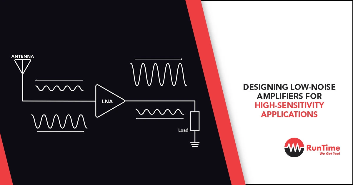
In RF receivers, LNAs amplify weak signals from antennas. A low noise figure is essential for maintaining signal integrity in noisy environments.
C. Scientific Instrumentation
Instruments like spectrometers and particle detectors rely on LNAs to amplify faint signals with minimal noise.
7. Advanced Topics in LNA Design
A. Cryogenic LNAs
For ultra-high-sensitivity applications, LNAs are cooled to cryogenic temperatures to reduce thermal noise. This is common in radio astronomy and quantum computing.
B. Wideband LNAs
Designing LNAs for wideband applications requires careful balancing of gain, noise, and impedance matching across a broad frequency range.
C. Integrated LNAs
Modern LNAs are often integrated into System-on-Chips (SoCs) or RFICs, requiring careful co-design with other components.
8. Best Practices for LNA Design
To summarize, here are the best practices for designing low-noise amplifiers:
- Start with a Clear Specification: Define the required gain, noise figure, bandwidth, and linearity.
- Choose the Right Components: Select low-noise transistors and passive components.
- Optimize the Topology: Use a topology that balances gain, noise, and stability.
- Simulate Thoroughly: Use simulation tools to validate the design before prototyping.
- Test Rigorously: Perform comprehensive testing to ensure performance meets specifications.
- Iterate and Improve: Use test results to refine the design and address any issues.
Conclusion
Designing low-noise amplifiers for high-sensitivity applications is a challenging but rewarding task for embedded engineers. By understanding the principles of noise, carefully selecting components, and optimizing the design, you can create LNAs that deliver exceptional performance in even the most demanding environments.
Whether you’re working on medical devices, wireless communication systems, or scientific instruments, mastering LNA design will enable you to push the boundaries of what’s possible in high-sensitivity applications. With the right tools, techniques, and attention to detail, you can achieve the low noise and high performance that your systems demand. Happy designing!


