Introduction
In the world of embedded systems, Printed Circuit Board (PCB) design is a critical aspect that can significantly impact the performance and reliability of the final product. One of the most common challenges faced by embedded engineers is managing signal integrity, particularly in long PCB traces.
Signal reflection issues in long traces can lead to data corruption, timing errors, and even complete system failure. Understanding and addressing these issues is essential for ensuring robust and reliable PCB designs.
This article delves into the causes of signal reflection in long PCB traces, the impact on system performance, and the strategies that embedded engineers can employ to mitigate these issues. By the end of this article, you will have a comprehensive understanding of how to design PCBs that minimize signal reflection and maintain signal integrity.
Understanding Signal Reflection
What is Signal Reflection?
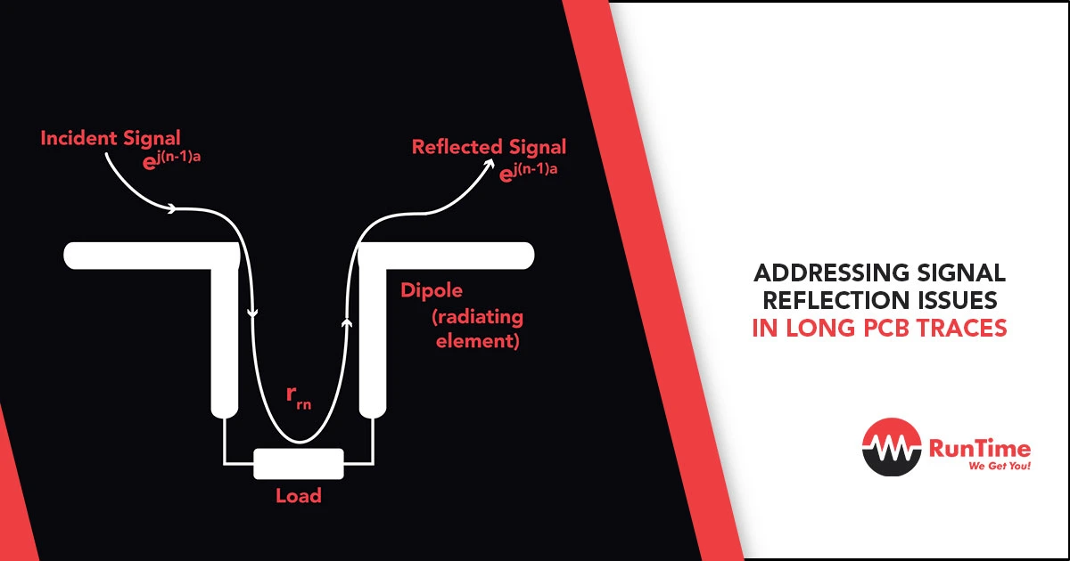
Signal reflection occurs when a signal traveling along a transmission line encounters an impedance mismatch. When this happens, a portion of the signal is reflected back towards the source, while the remainder continues to propagate towards the load. This reflected signal can interfere with the original signal, leading to distortions and errors.
Causes of Signal Reflection
Several factors can contribute to signal reflection in long PCB traces:
- Impedance Mismatch: The most common cause of signal reflection is an impedance mismatch between the transmission line and the load or source. If the impedance of the trace does not match the impedance of the connected components, signal reflection will occur.
- Trace Length: Long PCB traces are more susceptible to signal reflection due to the increased time it takes for the signal to travel the length of the trace. This can lead to significant phase differences between the incident and reflected signals.
- Termination: Improper termination of transmission lines can also cause signal reflection. Without proper termination, the signal can reflect off the open or shorted end of the trace.
- Via Stubs: Vias used to connect different layers of the PCB can act as stubs, causing impedance discontinuities and signal reflection.
Impact of Signal Reflection
Signal reflection can have several detrimental effects on the performance of an embedded system:
- Data Corruption: Reflected signals can interfere with the original signal, leading to data corruption and errors in communication.
- Timing Errors: Signal reflection can cause timing errors, particularly in high-speed digital systems. These errors can lead to incorrect data sampling and system malfunctions.
- Signal Integrity Degradation: Reflected signals can degrade the overall signal integrity, leading to reduced system performance and reliability.
- Electromagnetic Interference (EMI): Signal reflection can contribute to increased EMI, which can interfere with other components and systems.
Strategies for Addressing Signal Reflection
To mitigate signal reflection issues in long PCB traces, embedded engineers can employ several strategies. These strategies can be broadly categorized into impedance matching, termination techniques, trace routing, and design considerations.
1. Impedance Matching
Impedance matching is one of the most effective ways to minimize signal reflection. The goal is to ensure that the impedance of the transmission line matches the impedance of the source and load.
a. Controlled Impedance Traces
Controlled impedance traces are designed to have a specific impedance value, typically 50 ohms for single-ended signals and 100 ohms for differential pairs. This is achieved by carefully selecting the trace width, thickness, and dielectric material.
- Trace Width and Thickness: The width and thickness of the trace directly affect its impedance. Wider traces have lower impedance, while narrower traces have higher impedance. The thickness of the copper layer also plays a role.
- Dielectric Material: The dielectric constant of the PCB material affects the impedance. Materials with a lower dielectric constant result in higher impedance.
b. Impedance Calculators and Simulation Tools
Impedance calculators and simulation tools can help engineers design controlled impedance traces. These tools take into account the trace dimensions, dielectric properties, and other factors to calculate the impedance and ensure it matches the desired value.
- Impedance Calculators: Online impedance calculators can provide quick estimates of trace impedance based on input parameters.
- Simulation Tools: Advanced simulation tools, such as SPICE or electromagnetic field solvers, can provide more accurate impedance calculations and help optimize the trace design.
2. Termination Techniques
Proper termination of transmission lines is essential for minimizing signal reflection. Termination techniques ensure that the signal is absorbed at the load end, preventing it from reflecting back.
a. Series Termination
Series termination involves placing a resistor in series with the signal source. The resistor value is chosen to match the impedance of the transmission line.
- Advantages: Series termination is simple and effective for point-to-point connections.
- Disadvantages: It is less effective for multi-drop configurations, where multiple loads are connected to the same trace.
b. Parallel Termination
Parallel termination involves placing a resistor at the end of the transmission line, connected to ground or a reference voltage. The resistor value is chosen to match the impedance of the transmission line.
- Advantages: Parallel termination is effective for multi-drop configurations and can reduce signal reflection at the load end.
- Disadvantages: It can increase power consumption, as the termination resistor draws current from the signal source.
c. Thevenin Termination
Thevenin termination uses a voltage divider network to terminate the transmission line. Two resistors are connected in series between the supply voltage and ground, with the junction connected to the end of the transmission line.
- Advantages: Thevenin termination provides a good balance between impedance matching and power consumption.
- Disadvantages: It requires two resistors and can be more complex to implement.
d. AC Termination
AC termination involves placing a capacitor in series with the termination resistor. This allows the termination to be effective at high frequencies while minimizing DC power consumption.
- Advantages: AC termination is effective for high-speed signals and reduces DC power consumption.
- Disadvantages: It requires careful selection of the capacitor value to ensure proper termination.
3. Trace Routing
Proper trace routing is essential for minimizing signal reflection and maintaining signal integrity. The following techniques can help optimize trace routing:
a. Minimize Trace Length
Minimizing the length of PCB traces can reduce the likelihood of signal reflection. Shorter traces have less time for the signal to reflect back, reducing the impact on signal integrity.
- Component Placement: Careful placement of components can help minimize trace lengths. Place high-speed components closer to each other to reduce the distance signals need to travel.
- Layer Stacking: Use multiple PCB layers to route traces more efficiently. This can help reduce the overall trace length and minimize signal reflection.
b. Avoid Sharp Bends
Sharp bends in PCB traces can cause impedance discontinuities and signal reflection. Use gradual bends or curved traces to maintain consistent impedance.
- 45-Degree Bends: Use 45-degree bends instead of 90-degree bends to reduce impedance discontinuities.
- Curved Traces: Curved traces can provide a smoother transition and minimize signal reflection.
c. Differential Pair Routing
For high-speed differential signals, proper routing of differential pairs is essential. Ensure that the traces are routed closely together and maintain consistent spacing to minimize impedance mismatches.
- Length Matching: Ensure that the lengths of the differential pair traces are matched to avoid skew and signal reflection.
- Symmetrical Routing: Route the differential pair traces symmetrically to maintain consistent impedance and minimize signal reflection.
4. Design Considerations
In addition to impedance matching, termination, and trace routing, several design considerations can help minimize signal reflection in long PCB traces.
a. Via Design
Vias can introduce impedance discontinuities and signal reflection. Proper via design can help minimize these issues.
- Via Stubs: Minimize via stubs by using blind or buried vias. Stubless vias can reduce impedance discontinuities and signal reflection.
- Via Placement: Place vias carefully to avoid introducing unnecessary impedance mismatches. Use via stitching to maintain consistent impedance.
b. Ground Planes
Proper use of ground planes can help maintain consistent impedance and minimize signal reflection.
- Continuous Ground Planes: Use continuous ground planes to provide a low-impedance return path for signals. Avoid splitting ground planes, as this can introduce impedance discontinuities.
- Ground Plane Clearance: Ensure adequate clearance between signal traces and ground planes to maintain consistent impedance.
c. Signal Integrity Analysis
Signal integrity analysis is essential for identifying and addressing potential signal reflection issues. Use simulation tools to analyze the signal integrity of your PCB design.
- Time-Domain Reflectometry (TDR): TDR analysis can help identify impedance mismatches and signal reflection points in your PCB design.
- Eye Diagram Analysis: Eye diagram analysis can provide insights into the quality of high-speed signals and help identify signal integrity issues.
Case Study: Addressing Signal Reflection in a High-Speed Communication PCB
To illustrate the practical application of these strategies, let’s consider a case study of a high-speed communication PCB design.
Application Overview
The PCB is designed for a high-speed communication system, with data rates of up to 10 Gbps. The design includes multiple long traces for high-speed differential pairs, as well as single-ended signals.
Challenges
The primary challenges in this design are:
- Signal Reflection: Long traces for high-speed differential pairs are susceptible to signal reflection, which can lead to data corruption and timing errors.
- Impedance Matching: Ensuring consistent impedance for the differential pairs and single-ended signals is critical for maintaining signal integrity.
- Termination: Proper termination of the high-speed signals is essential to minimize signal reflection.
Strategies Employed
To address these challenges, the following strategies were employed:
- Controlled Impedance Traces: The differential pairs were designed with controlled impedance of 100 ohms, while the single-ended signals were designed with 50-ohm impedance. The trace width, thickness, and dielectric material were carefully selected to achieve the desired impedance.
- Series Termination: Series termination resistors were used for the single-ended signals to match the impedance of the transmission line. The resistor values were chosen to minimize signal reflection.
- Differential Pair Routing: The differential pairs were routed closely together with consistent spacing. Length matching was used to ensure that the traces were of equal length, minimizing skew and signal reflection.
- Via Design: Blind vias were used to minimize via stubs and reduce impedance discontinuities. Vias were placed carefully to avoid introducing unnecessary impedance mismatches.
- Ground Planes: Continuous ground planes were used to provide a low-impedance return path for the signals. Adequate clearance was maintained between the signal traces and ground planes to ensure consistent impedance.
- Signal Integrity Analysis: TDR and eye diagram analysis were used to identify and address potential signal reflection issues. The simulation results were used to optimize the trace design and termination.
Results
By implementing these strategies, the high-speed communication PCB design achieved the following results:
- Minimized Signal Reflection: The controlled impedance traces and proper termination techniques minimized signal reflection, ensuring robust signal integrity.
- Consistent Impedance: The careful design of the differential pairs and single-ended signals ensured consistent impedance, reducing the likelihood of signal reflection.
- High-Speed Performance: The optimized trace routing and via design allowed the PCB to achieve the required data rates of up to 10 Gbps without significant signal integrity issues.
Conclusion
Addressing signal reflection issues in long PCB traces is a critical aspect of embedded systems design. By understanding the causes of signal reflection and employing strategies such as impedance matching, proper termination, optimized trace routing, and careful design considerations, embedded engineers can minimize signal reflection and maintain signal integrity.
As the demand for high-speed and high-performance embedded systems continues to grow, the importance of robust PCB design practices will only increase. By staying informed and proactive, embedded engineers can ensure the success of their designs and deliver reliable and high-performance products.


