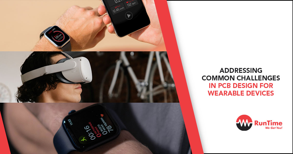
Introduction
Wearable devices have become an integral part of our daily lives, from fitness trackers and smartwatches to medical monitoring devices and augmented reality glasses. These devices are designed to be compact, lightweight, and energy-efficient, making them highly portable and user-friendly. However, designing printed circuit boards (PCBs) for wearable devices presents a unique set of challenges that embedded engineers must navigate to ensure optimal performance, reliability, and user experience.
In this article, we will explore the common challenges in PCB design for wearable devices and provide practical solutions to address these issues. By understanding and overcoming these challenges, embedded engineers can create innovative and high-performing wearable devices that meet the demands of today’s tech-savvy consumers.
1. Miniaturization and Space Constraints
Challenge:
One of the most significant challenges in designing PCBs for wearable devices is the need for miniaturization. Wearable devices are typically small and lightweight, requiring PCBs to be compact and densely packed with components. This space constraint can make it difficult to accommodate all necessary components, routing, and connections while maintaining signal integrity and thermal management.
Solution:
To address the challenge of miniaturization, embedded engineers can employ several strategies:
- High-Density Interconnect (HDI) PCBs: HDI PCBs use advanced manufacturing techniques to create finer traces and smaller vias, allowing for higher component density and more efficient use of space. This technology enables the design of compact PCBs without compromising performance.
- Component Selection: Choose smaller, surface-mount components that take up less space on the PCB. Consider using chip-scale packages (CSPs) and ball grid arrays (BGAs) to reduce the footprint of critical components.
- Flexible and Rigid-Flex PCBs: Flexible and rigid-flex PCBs offer greater design flexibility, allowing engineers to bend and fold the PCB to fit within the device’s form factor. This approach can save space and enable more creative designs.
- 3D PCB Design: Utilize 3D PCB design tools to visualize and optimize the placement of components in three dimensions. This can help identify potential space-saving opportunities and ensure that all components fit within the device’s enclosure.
2. Power Management and Energy Efficiency
Challenge:
Wearable devices are often powered by small batteries, making power management and energy efficiency critical considerations in PCB design. Engineers must design PCBs that minimize power consumption while maintaining the device’s functionality and performance.
Solution:
To optimize power management and energy efficiency, consider the following approaches:
- Low-Power Components: Select low-power microcontrollers, sensors, and other components that consume minimal energy during operation. Look for components with sleep modes and power-saving features.
- Power Management ICs (PMICs): Integrate PMICs into the PCB design to efficiently regulate and distribute power to different components. PMICs can help extend battery life by optimizing power usage and reducing energy waste.
- Energy Harvesting: Explore energy harvesting techniques, such as solar cells, thermoelectric generators, or kinetic energy harvesters, to supplement the device’s power supply. This can reduce the reliance on batteries and extend the device’s operational life.
- Efficient PCB Layout: Design the PCB layout to minimize power losses and optimize signal integrity. Use shorter traces, reduce parasitic capacitance, and avoid unnecessary power-hungry components.
3. Signal Integrity and EMI/EMC Compliance
Challenge:
Wearable devices often operate in environments with high levels of electromagnetic interference (EMI), which can affect signal integrity and device performance. Ensuring electromagnetic compatibility (EMC) is essential to meet regulatory standards and prevent interference with other devices.
Solution:
To maintain signal integrity and achieve EMI/EMC compliance, embedded engineers can implement the following strategies:
- Proper Grounding and Shielding: Design a solid ground plane and use shielding techniques to minimize EMI. Ensure that sensitive components and traces are adequately shielded from external interference.
- Differential Signaling: Use differential signaling for high-speed data transmission to reduce noise and improve signal integrity. Differential pairs can help cancel out common-mode noise and enhance signal quality.
- EMI Filters: Incorporate EMI filters into the PCB design to suppress unwanted noise and interference. These filters can be placed at the input and output of power supplies and signal lines.
- Compliance Testing: Conduct thorough EMI/EMC testing during the design and prototyping phases to identify and address potential issues early. Ensure that the device meets relevant regulatory standards, such as FCC, CE, and IEC.
4. Thermal Management
Challenge:
Wearable devices generate heat during operation, and the compact nature of these devices can make thermal management challenging. Excessive heat can degrade component performance, reduce battery life, and cause discomfort to the user.
Solution:
To effectively manage heat in wearable devices, consider the following thermal management techniques:
- Thermal Vias: Use thermal vias to dissipate heat from high-power components to the PCB’s inner layers or external heat sinks. Thermal vias can help distribute heat more evenly and prevent hot spots.
- Heat Spreaders and Heat Sinks: Integrate heat spreaders or heat sinks into the PCB design to absorb and dissipate heat. These components can be made from materials with high thermal conductivity, such as copper or aluminum.
- Component Placement: Carefully place heat-generating components to avoid concentration of heat in one area. Distribute these components across the PCB to promote better heat dissipation.
- Thermal Simulation: Use thermal simulation tools to analyze the PCB’s thermal performance and identify potential hotspots. This can help optimize the design for better heat management.
5. Durability and Reliability
Challenge:
Wearable devices are subjected to various environmental stresses, such as moisture, temperature fluctuations, and mechanical shocks. Ensuring the durability and reliability of the PCB is crucial to the device’s longevity and performance.
Solution:
To enhance the durability and reliability of PCBs for wearable devices, consider the following approaches:
- Conformal Coating: Apply conformal coating to the PCB to protect it from moisture, dust, and other environmental contaminants. Conformal coatings can also provide additional mechanical protection.
- Robust Materials: Use high-quality, durable materials for the PCB and components. Consider using flexible PCBs made from polyimide or other robust materials that can withstand bending and flexing.
- Environmental Testing: Conduct environmental testing, such as thermal cycling, humidity testing, and vibration testing, to ensure the PCB can withstand real-world conditions. This can help identify potential weaknesses and improve the design.
- Mechanical Design: Design the device’s enclosure and PCB layout to minimize mechanical stress on the components. Use strain relief techniques for connectors and cables to prevent damage during use.
6. User Comfort and Ergonomics
Challenge:
Wearable devices are worn on the body, making user comfort and ergonomics critical considerations in PCB design. The PCB must be designed to fit comfortably within the device’s form factor without causing discomfort or irritation to the user.
Solution:
To ensure user comfort and ergonomics, embedded engineers can take the following steps:
- Flexible PCBs: Use flexible PCBs that can conform to the shape of the device and the user’s body. Flexible PCBs can reduce the risk of discomfort and improve the overall user experience.
- Lightweight Design: Minimize the weight of the PCB and components to reduce the overall weight of the device. Lightweight wearables are more comfortable to wear for extended periods.
- Smooth Edges and Rounded Corners: Design the PCB and enclosure with smooth edges and rounded corners to prevent irritation and ensure a comfortable fit.
- User Testing: Conduct user testing to gather feedback on the device’s comfort and ergonomics. Use this feedback to make iterative improvements to the design.
7. Manufacturing and Assembly Challenges
Challenge:
The small size and complexity of PCBs for wearable devices can pose challenges during manufacturing and assembly. Ensuring high-quality production and assembly is essential to avoid defects and ensure the device’s reliability.
Solution:
To address manufacturing and assembly challenges, consider the following strategies:
- Design for Manufacturability (DFM): Follow DFM guidelines to ensure the PCB design is optimized for manufacturing. This includes considering factors such as component placement, trace width, and solder mask design.
- Advanced Manufacturing Techniques: Utilize advanced manufacturing techniques, such as laser drilling and automated optical inspection (AOI), to achieve high precision and quality in PCB production.
- Collaboration with Manufacturers: Work closely with PCB manufacturers and assembly partners to address potential issues early in the design process. Collaborate on design reviews and prototyping to ensure a smooth transition to production.
- Quality Control: Implement rigorous quality control processes during manufacturing and assembly to detect and address defects. Use testing and inspection methods, such as X-ray inspection and functional testing, to ensure the PCB meets quality standards.
Conclusion
Designing PCBs for wearable devices presents a unique set of challenges that require innovative solutions and careful consideration of various factors, including miniaturization, power management, signal integrity, thermal management, durability, user comfort, and manufacturing. By addressing these challenges head-on and implementing the strategies outlined in this article, embedded engineers can create high-performing, reliable, and user-friendly wearable devices that meet the demands of today’s consumers.
As the wearable technology market continues to grow, the importance of effective PCB design cannot be overstated. By staying informed about the latest advancements in PCB technology and continuously refining their design practices, embedded engineers can push the boundaries of what’s possible in wearable devices and contribute to the development of cutting-edge products that enhance our daily lives.
In the end, the success of a wearable device hinges on the quality of its PCB design. By overcoming the common challenges and delivering innovative solutions, embedded engineers can play a pivotal role in shaping the future of wearable technology.


