The embedded systems landscape is on the cusp of a profound transformation, driven by an innovation that promises to redefine how we conceive, design, and manufacture electronic devices: the chiplet. For decades, the industry has largely adhered to the monolithic System-on-Chip (SoC) paradigm, integrating an ever-increasing array of functionalities onto a single silicon die. While this approach has yielded incredible advancements, it is now confronting formidable challenges in terms of escalating design complexity, diminishing returns from Moore’s Law, ballooning manufacturing costs, and rigid design flexibility.
Enter chiplets. These small, specialized silicon dies, each performing a specific function, are poised to disaggregate the traditional SoC, ushering in an era of modular processors. By allowing engineers to mix and match pre-verified, optimized chiplets from various manufacturers, this revolutionary approach is not merely an incremental improvement; it represents a fundamental shift in design paradigms that will profoundly impact embedded engineers across all sectors, from industrial IoT and automotive to edge AI and consumer electronics.
The Looming Crisis of Monolithic SoCs and the Genesis of Chiplets
For much of the semiconductor industry’s history, the relentless march of Moore’s Law—the observation that the number of transistors on an integrated circuit doubles approximately every two years—has been the guiding principle. This scaling allowed for ever-more complex and powerful SoCs to be fabricated on a single piece of silicon. However, as process nodes shrink to the sub-7nm and even 3nm realms, the challenges associated with monolithic designs have intensified dramatically:
- Escalating Manufacturing Costs and Diminishing Yields: Fabricating large, cutting-edge monolithic dies is incredibly expensive. Even a single microscopic defect can render an entire complex SoC unusable, leading to significantly reduced yields and astronomical development costs. Smaller chiplets, by contrast, exhibit higher yields, as the probability of a defect on a smaller die is lower.
- Design Complexity and Verification Headaches: As more IP blocks are crammed onto a single die, the complexity of design, integration, and, crucially, verification becomes an almost insurmountable hurdle. Simulating and verifying the interactions of hundreds of millions, or even billions, of transistors and diverse IP cores is a time-consuming and error-prone process.
- Thermal Management Challenges: Packing immense computational power into a confined area on a single die generates significant heat, necessitating complex and often power-hungry thermal management solutions.
- Lack of Flexibility and IP Reuse: Once a monolithic SoC is designed and fabricated, it offers limited flexibility for customization or upgrades. Moreover, reusing specific IP blocks often requires a complete re-spin of the entire SoC, incurring substantial costs and delays.
- Process Node Optimization: Not all functionalities within an SoC require the most advanced process node. For instance, high-speed logic benefits from advanced nodes, while analog components or I/O interfaces might be more cost-effectively produced on older, more mature processes. Monolithic designs force all components onto the same process, leading to compromises in performance or cost efficiency.
These mounting pressures have spurred the industry to seek alternative architectures, leading to the re-emergence and rapid advancement of chiplet technology. While the concept of multi-chip modules has existed for decades, modern chiplets leverage sophisticated inter-chiplet communication standards and advanced packaging techniques to achieve near-monolithic performance and integration density.
The Modular Promise: Advantages of Chiplets for Embedded Systems
The transition to a chiplet-based paradigm offers a compelling array of advantages for embedded engineers, fundamentally altering how systems are architected and implemented:
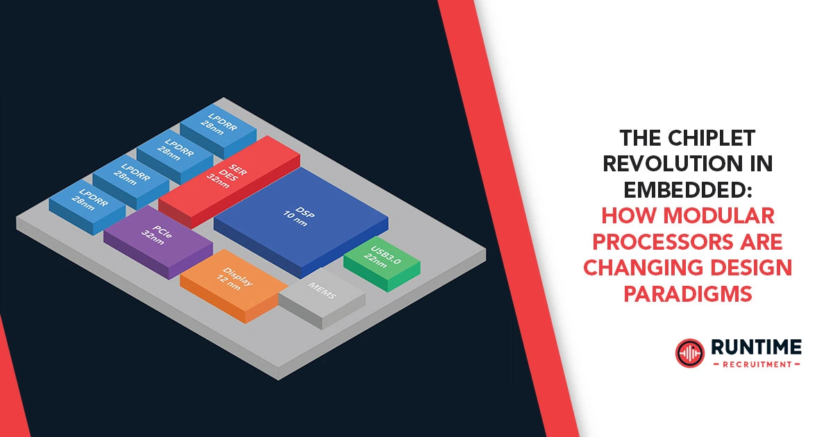
- Enhanced Scalability and Customization: Chiplets enable a truly modular approach to system design. Instead of designing a new SoC from scratch for each application, engineers can select from a library of pre-designed, pre-verified chiplets—such as CPU cores, GPU accelerators, memory controllers, AI/ML inference engines, specialized I/O modules, and connectivity interfaces (e.g., 5G, Wi-Fi 6E). This “Lego-block” approach allows for highly customized solutions tailored to specific performance, power, and cost requirements, accelerating time-to-market significantly. Imagine an industrial IoT gateway that can be precisely configured with the right processing power, sensor interfaces, and network connectivity simply by swapping out chiplets.
- Improved Yields and Reduced Costs: As mentioned, smaller dies inherently have higher manufacturing yields. By breaking a large SoC into smaller chiplets, the overall manufacturing cost can be reduced due to fewer defective units. Furthermore, the ability to mix and match chiplets manufactured on different process nodes optimizes cost efficiency. For example, a high-performance CPU chiplet might be fabricated on a bleeding-edge 3nm process, while a less performance-critical I/O chiplet could be built on a more cost-effective 28nm or 40nm process, minimizing the overall silicon cost.
- Accelerated Time-to-Market and IP Reuse: The reusability of pre-qualified chiplets dramatically shrinks development cycles. Instead of lengthy design and verification phases for an entire SoC, engineers can focus on integrating existing chiplets and developing application-specific software. This fosters a vibrant ecosystem of IP vendors offering specialized chiplets, much like the software component market.
- Heterogeneous Integration for Optimal Performance and Power: Chiplets facilitate heterogeneous integration, allowing different functional blocks to be optimized independently. A memory chiplet might be optimized for density and bandwidth, a neural processing unit (NPU) for AI inference efficiency, and a security chiplet for robust cryptographic operations. This tailored optimization at the chiplet level translates to superior system-level performance and reduced power consumption compared to monolithic designs where compromises are often made to fit everything onto one die. This is particularly critical for power-constrained embedded applications at the edge.
- Mitigation of Moore’s Law Limitations: As the physical limits of transistor scaling become increasingly apparent, chiplets offer a pathway to continued performance improvements. Instead of relying solely on shrinking transistors, performance gains can be achieved through advanced packaging techniques (e.g., 2.5D and 3D stacking) that bring chiplets closer together, reducing interconnect latency and increasing bandwidth.
- Supply Chain Flexibility and Resilience: Chiplets can be sourced from multiple foundries and vendors, reducing reliance on a single manufacturing pipeline. This diversification enhances supply chain resilience, a lesson keenly learned during recent global events.
Navigating the New Terrain: Challenges and Considerations for Embedded Engineers
While the benefits of chiplets are compelling, their adoption in embedded systems is not without its challenges. Embedded engineers must adapt their skillsets and design methodologies to navigate this new landscape:
- Inter-Chiplet Communication and Interoperability: The efficacy of chiplet-based designs hinges on robust, high-speed, and standardized communication interfaces between the individual dies. Initiatives like the Universal Chiplet Interconnect Express (UCIe) standard are crucial in this regard, aiming to establish an open ecosystem where chiplets from different vendors can seamlessly interoperate. However, engineers will need to deeply understand the nuances of these interconnects, including bandwidth, latency, power consumption, and error correction mechanisms. This requires a shift from traditional on-die communication analysis to a more system-level perspective encompassing die-to-die interfaces.
- Advanced Packaging Technologies: Chiplets necessitate sophisticated packaging techniques beyond conventional 2D planar integration. Technologies like 2.5D (using silicon interposers) and 3D stacking (Through-Silicon Vias – TSVs) are essential for achieving the required density and low-latency communication. Embedded engineers will need to collaborate closely with packaging experts and understand the thermal, mechanical, and electrical implications of these advanced packaging solutions.
- Thermal Management Across Multiple Dies: While smaller chiplets generate less heat individually, the dense integration of multiple chiplets within a single package can concentrate heat, posing significant thermal management challenges. Designing effective cooling solutions that consider heat dissipation across various chiplets with potentially different power profiles will be paramount.
- System-Level Verification and Testing: Verifying the functionality and reliability of a system composed of multiple chiplets from potentially different vendors introduces new complexities. Traditional verification methodologies designed for monolithic SoCs may not be sufficient. New approaches are needed to ensure end-to-end system performance, address signal integrity across chiplet boundaries, and validate the correct operation of diverse IP blocks in concert. This will involve more rigorous simulation, emulation, and validation strategies.
- Power Delivery and Management: Distributing power efficiently and reliably across multiple chiplets, each with its own voltage and current requirements, adds another layer of complexity. Dynamic voltage and frequency scaling (DVFS) across chiplets will require sophisticated power management unit (PMU) designs and control algorithms.
- Tooling and Design Flows: The existing Electronic Design Automation (EDA) toolchain, largely optimized for monolithic designs, needs to evolve to fully support chiplet-based architectures. New tools are required for heterogeneous integration, multi-die floorplanning, inter-chiplet routing, thermal analysis, and holistic system-level simulation. Collaboration between EDA vendors, IP providers, and semiconductor companies will be vital in developing these advanced design flows.
- Supply Chain and Ecosystem Management: The chiplet revolution necessitates a more fragmented yet interconnected supply chain. Embedded engineers will be part of a broader ecosystem, sourcing chiplets from various providers. This requires robust quality control, standardized interfaces, and strong collaborative partnerships. The concept of a “chiplet marketplace” where readily available, pre-certified chiplets can be easily procured is a significant driver for widespread adoption.
- Security Considerations: With multiple chiplets potentially sourced from different vendors, ensuring end-to-end security becomes even more critical. New security paradigms are needed to protect against malicious chiplets, ensure secure inter-chiplet communication, and maintain the integrity of the overall system.
The Future of Embedded Design: A Modular Horizon
The chiplet revolution is not a distant fantasy; it is already underway, spearheaded by industry leaders like AMD, Intel, and NVIDIA in high-performance computing. However, its impact on embedded systems, while perhaps arriving slightly later, promises to be equally transformative. We can anticipate several key trends shaping the future of embedded design:
- Democratization of Advanced Silicon: Chiplets will make cutting-edge silicon technology more accessible to a wider range of companies, including smaller players and startups in the embedded space. By leveraging off-the-shelf chiplets, companies can innovate without the prohibitive costs and risks associated with full SoC development.
- Specialized Embedded Accelerators: The modularity of chiplets will accelerate the development and integration of highly specialized accelerators for embedded applications, such as ultra-low-power AI inference engines for edge devices, highly efficient video processing units for smart cameras, or dedicated security modules for critical infrastructure.
- Increased Focus on Software-Defined Hardware: As hardware becomes more modular, the importance of software for orchestrating and managing the interactions between chiplets will grow. Embedded engineers will increasingly work at a higher level of abstraction, leveraging software to define and optimize system behavior.
- The Rise of System Integrators (for hardware): Just as software integrators assemble components from various sources, a new breed of “hardware system integrators” may emerge, specializing in selecting, integrating, and validating chiplets from different vendors to create optimized embedded solutions.
- New Business Models: The chiplet ecosystem will foster new business models, including chiplet IP licensing, chiplet-as-a-service, and specialized design services for modular embedded systems.
For embedded engineers, this paradigm shift represents both a challenge and an immense opportunity. Those who embrace the principles of modular design, master advanced packaging considerations, and adapt to new verification and integration methodologies will be at the forefront of innovation. The ability to abstract away the complexities of monolithic design and instead focus on the optimal composition and interaction of specialized functional blocks will be a highly sought-after skill. The future of embedded systems is undeniably modular, and the chiplet revolution is the catalyst for this exciting new era of design.


