Introduction
In the realm of high-speed PCB design, maintaining signal integrity is paramount. As data rates continue to climb, the challenges associated with signal integrity become increasingly complex. One of the most effective techniques for ensuring robust signal integrity in high-speed designs is the use of differential pair routing. Differential pairs are used extensively in high-speed communication protocols such as USB, HDMI, PCIe, and Ethernet, among others.
This article aims to provide embedded engineers with a comprehensive understanding of differential pair routing, its benefits, and the best practices for implementing it in high-speed PCB designs. By the end of this article, you will have a solid grasp of how to design and route differential pairs to maintain signal integrity and achieve optimal performance in your high-speed PCB designs.
What are Differential Pairs?
Definition and Basic Concepts
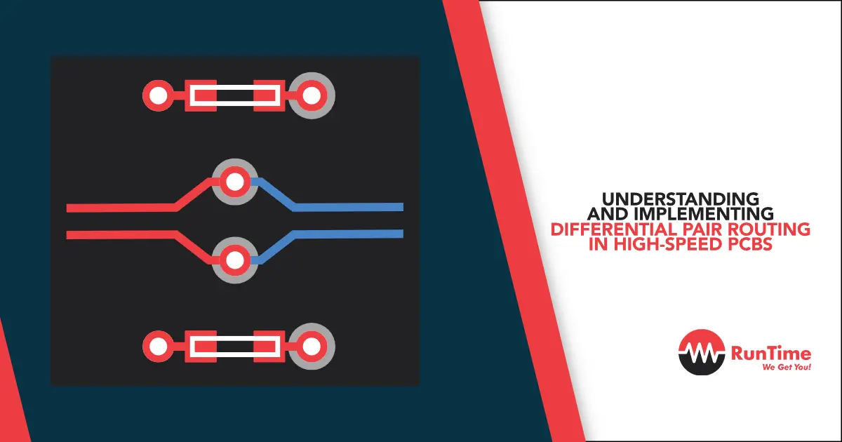
A differential pair consists of two conductors (traces) that carry equal and opposite signals. The signal of interest is the difference between the two conductors, rather than the absolute voltage on either conductor. This differential signaling offers several advantages over single-ended signaling, particularly in high-speed applications.
Advantages of Differential Pair Routing
- Noise Immunity: Differential pairs are highly immune to common-mode noise. Since both conductors are exposed to the same noise, the differential receiver can effectively cancel out the noise by subtracting the two signals.
- Reduced Electromagnetic Interference (EMI): The equal and opposite currents in the two conductors generate electromagnetic fields that tend to cancel each other out, reducing EMI.
- Improved Signal Integrity: Differential signaling helps maintain signal integrity over longer distances and at higher data rates compared to single-ended signaling.
- Lower Voltage Swing: Differential signaling can achieve the same signal-to-noise ratio (SNR) with a lower voltage swing, reducing power consumption.
Key Parameters in Differential Pair Routing
To effectively implement differential pair routing, it is essential to understand and control several key parameters:
1. Differential Impedance
Differential impedance (Zdiff) is the impedance seen by the differential signal as it travels along the pair of conductors. It is a critical parameter that must be carefully controlled to ensure proper signal transmission.
- Calculating Differential Impedance: The differential impedance depends on the trace width, spacing between the traces, dielectric constant of the PCB material, and the height of the traces above the ground plane. Impedance calculators and simulation tools can help determine the appropriate trace dimensions to achieve the desired differential impedance.
- Common Values: Typical differential impedance values are 90 ohms for USB and 100 ohms for Ethernet and PCIe.
2. Common-Mode Impedance
Common-mode impedance (Zcm) is the impedance seen by common-mode signals (signals that are in phase on both conductors). While differential signals are the primary focus, controlling common-mode impedance is also important for minimizing common-mode noise and EMI.
3. Skew
Skew refers to the difference in propagation delay between the two conductors of a differential pair. Excessive skew can degrade signal integrity and lead to errors in the received signal.
- Minimizing Skew: To minimize skew, ensure that the lengths of the two traces are matched as closely as possible. This can be achieved through careful routing and the use of length-matching techniques.
4. Crosstalk
Crosstalk is the unwanted coupling of signals between adjacent traces. In high-speed designs, crosstalk can significantly impact signal integrity.
- Reducing Crosstalk: To reduce crosstalk, maintain adequate spacing between differential pairs and other traces. Use ground planes and guard traces to provide shielding between sensitive signals.
Best Practices for Differential Pair Routing
Implementing differential pair routing requires careful attention to detail and adherence to best practices. The following sections outline the key considerations and techniques for successful differential pair routing.
1. Trace Width and Spacing
The width of the traces and the spacing between them are critical factors in achieving the desired differential impedance.
- Trace Width: The width of the traces should be chosen based on the desired impedance and the PCB manufacturing capabilities. Wider traces have lower impedance, while narrower traces have higher impedance.
- Spacing: The spacing between the traces affects the coupling between them. Closer spacing increases coupling and reduces differential impedance, while wider spacing decreases coupling and increases differential impedance.
2. Length Matching
Length matching is essential for minimizing skew and ensuring that the differential signals arrive at the receiver simultaneously.
- Manual Length Matching: Manually adjust the lengths of the traces by adding meanders or serpentine routing to the shorter trace. Ensure that the meanders are smooth and do not introduce sharp bends.
- Automatic Length Matching: Many PCB design tools offer automatic length-matching features that can adjust the trace lengths to meet specified tolerances.
3. Routing Topology
The routing topology refers to the physical layout of the differential pairs on the PCB. Proper routing topology is crucial for maintaining signal integrity.
- Point-to-Point Routing: For simple point-to-point connections, route the differential pairs directly from the transmitter to the receiver. Ensure that the traces are routed closely together and maintain consistent spacing.
- Multi-Drop Routing: For multi-drop configurations, where multiple receivers are connected to the same differential pair, use a daisy-chain topology. Ensure that the stubs (short branches to the receivers) are as short as possible to minimize reflections.
4. Via Design
Vias are necessary for routing differential pairs between different layers of the PCB. However, vias can introduce impedance discontinuities and signal reflections.
- Minimizing Via Stubs: Use blind or buried vias to minimize via stubs. Stubless vias can reduce impedance discontinuities and signal reflections.
- Via Placement: Place vias carefully to avoid introducing unnecessary impedance mismatches. Use via stitching to maintain consistent impedance.
5. Ground Planes
Ground planes play a crucial role in maintaining consistent impedance and providing a low-impedance return path for the differential signals.
- Continuous Ground Planes: Use continuous ground planes to provide a low-impedance return path for the signals. Avoid splitting ground planes, as this can introduce impedance discontinuities.
- Ground Plane Clearance: Ensure adequate clearance between the differential pairs and the ground planes to maintain consistent impedance.
6. Termination
Proper termination of differential pairs is essential for minimizing signal reflections and ensuring proper signal transmission.
- Differential Termination: Use differential termination resistors at the receiver end to match the differential impedance of the transmission line. The resistor value should be equal to the differential impedance (e.g., 100 ohms for Ethernet).
- AC Termination: For high-speed signals, consider using AC termination (a capacitor in series with the termination resistor) to reduce DC power consumption while maintaining proper termination at high frequencies.
7. Signal Integrity Analysis
Signal integrity analysis is essential for identifying and addressing potential issues in the differential pair routing.
- Time-Domain Reflectometry (TDR): TDR analysis can help identify impedance mismatches and signal reflection points in the differential pairs.
- Eye Diagram Analysis: Eye diagram analysis can provide insights into the quality of the differential signals and help identify signal integrity issues.
Case Study: Implementing Differential Pair Routing in a High-Speed Ethernet PCB
To illustrate the practical application of differential pair routing, let’s consider a case study of a high-speed Ethernet PCB design.
Application Overview
The PCB is designed for a high-speed Ethernet interface, with data rates of up to 10 Gbps. The design includes multiple differential pairs for the Ethernet signals, as well as other high-speed signals.
Challenges
The primary challenges in this design are:
- Differential Impedance Control: Ensuring consistent differential impedance of 100 ohms for the Ethernet differential pairs.
- Length Matching: Minimizing skew by matching the lengths of the differential pairs.
- Crosstalk: Reducing crosstalk between the differential pairs and other high-speed signals.
- Termination: Properly terminating the differential pairs to minimize signal reflections.
Strategies Employed
To address these challenges, the following strategies were employed:
- Controlled Impedance Traces: The differential pairs were designed with controlled impedance of 100 ohms. The trace width and spacing were carefully selected to achieve the desired impedance.
- Length Matching: The lengths of the differential pairs were matched using manual length-matching techniques. Meanders were added to the shorter traces to ensure equal lengths.
- Crosstalk Reduction: Adequate spacing was maintained between the differential pairs and other high-speed signals. Ground planes and guard traces were used to provide shielding and reduce crosstalk.
- Via Design: Blind vias were used to minimize via stubs and reduce impedance discontinuities. Vias were placed carefully to avoid introducing unnecessary impedance mismatches.
- Ground Planes: Continuous ground planes were used to provide a low-impedance return path for the differential signals. Adequate clearance was maintained between the differential pairs and the ground planes.
- Termination: Differential termination resistors of 100 ohms were used at the receiver end to match the differential impedance of the transmission line.
- Signal Integrity Analysis: TDR and eye diagram analysis were used to identify and address potential signal integrity issues. The simulation results were used to optimize the differential pair routing.
Results
By implementing these strategies, the high-speed Ethernet PCB design achieved the following results:
- Consistent Differential Impedance: The controlled impedance traces ensured consistent differential impedance of 100 ohms, minimizing signal reflections.
- Minimized Skew: The length-matching techniques minimized skew, ensuring that the differential signals arrived at the receiver simultaneously.
- Reduced Crosstalk: The adequate spacing and use of ground planes and guard traces reduced crosstalk, improving signal integrity.
- Proper Termination: The differential termination resistors minimized signal reflections, ensuring proper signal transmission.
- High-Speed Performance: The optimized differential pair routing allowed the PCB to achieve the required data rates of up to 10 Gbps without significant signal integrity issues.
Conclusion
Differential pair routing is a critical technique for maintaining signal integrity in high-speed PCB designs. By understanding the key parameters and adhering to best practices, embedded engineers can effectively implement differential pair routing and achieve optimal performance in their high-speed designs.
As the demand for high-speed and high-performance embedded systems continues to grow, the importance of robust PCB design practices will only increase. By staying informed and proactive, embedded engineers can ensure the success of their designs and deliver reliable and high-performance products.


