Managing multiple clock domains in FPGA designs is a critical aspect of digital design that requires careful consideration and adherence to best practices. Clock domain crossings are a common source of bugs and can significantly impact the performance and reliability of an FPGA design. In this context, understanding the challenges associated with multiple clock domains and adopting proven strategies for managing them is essential for successful implementation.
This introduction will delve into the key principles and techniques that engineers can employ to effectively handle multiple clock domains in FPGA designs, ensuring synchronization, minimizing metastability issues, and optimizing overall system performance. By exploring best practices in clock domain crossing design, this discussion aims to provide valuable insights and practical recommendations for engineers working on complex FPGA projects.
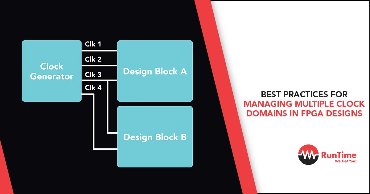
Clock Domain Crossing in FPGA Design
Clock Domain Crossing (CDC) is a critical aspect of FPGA design, ensuring proper data transfer between different clock domains. When signals from one clock domain interact with another, it can lead to issues such as metastability, data loss, or functional failures.
To address these challenges, engineers utilize synchronization techniques like 2-flop synchronizers or Gray coding. The risks associated with CDC, including timing violations and system crashes, highlight the importance of thorough timing analysis and robust design practices. Mitigating CDC risks requires a meticulous approach to synchronization and a deep understanding of the design’s timing constraints.
Understanding CDC
Clock Domain Crossing is a fundamental concept in digital design, particularly in Field-Programmable Gate Arrays (FPGAs). In modern electronic systems, where multiple clock domains exist, ensuring that data transfers between these domains occur reliably and without errors is paramount. The heart of CDC lies in the fact that when a signal transitions from one clock domain to another, there exists a possibility of metastability, a state where the receiving flip-flop fails to settle to a valid logic level within the required setup time, leading to unpredictable behavior.
Synchronization Techniques
One common method employed to tackle metastability issues is the use of 2-flop synchronizers. These synchronizers consist of two flip-flops in series, which helps in reducing the probability of metastability to an extremely low level. Another technique often used is Gray coding, which ensures that only one bit changes between consecutive states, minimizing the chances of misinterpretation during the transition.
Consequences of Inadequate CDC Handling
The consequences of failing to address CDC properly can be severe. Timing violations can result in incorrect data being captured or transmitted, leading to system malfunctions or crashes. Therefore, FPGA designers must conduct rigorous timing analysis to identify and rectify potential CDC hazards early in the design phase. Additionally, adopting robust design practices, such as clock domain isolation and proper signal synchronization, is crucial for overall system reliability.
Mitigating CDC Risks
Mitigating CDC risks demands a comprehensive understanding of the system’s clocking architecture and timing constraints. Engineers need to carefully plan the synchronization logic, ensure proper clock domain crossing protocols, and validate the design through simulations and formal verification methods. By incorporating these practices, FPGA designers can enhance the reliability and performance of their designs, ultimately leading to successful implementation and operation of complex electronic systems.
Challenges in Managing Multiple Clock Domains
Clock Domain Synchronization Hurdles
In modern digital design, managing multiple clock domains is a common challenge. Ensuring that signals crossing between these domains are properly synchronized is crucial to prevent issues such as metastability. This section will delve into the complexities of clock domain synchronization and strategies to mitigate related risks.
Timing Closure Difficulties
Another significant challenge in dealing with multiple clock domains is achieving timing closure. With each clock domain operating independently, meeting timing constraints becomes more intricate. Factors such as clock skew and data transfer between domains can complicate the timing analysis process. This part of the blog will explore the various obstacles faced in achieving timing closure and offer insights into addressing these difficulties.
Strategies for Clock Domain Synchronization
To address the synchronization hurdles associated with multiple clock domains, designers often employ techniques such as synchronization circuits, two-flop synchronizers, and handshake protocols. Understanding the trade-offs between synchronization overhead and performance is crucial in selecting the most suitable synchronization mechanism for a given design. This section will discuss these strategies in detail and highlight their impact on design robustness and performance.
Optimizing Timing Closure
In the realm of timing closure difficulties, optimizing design constraints, clock tree synthesis, and physical design considerations play pivotal roles. Advanced timing analysis tools, like static timing analysis and delay calculation, aid in identifying critical paths and optimizing timing paths across different clock domains. Exploring methods to minimize clock skew, address setup and hold time violations, and fine-tune the design for improved timing closure will be key focal points in this segment.
Challenges of Asynchronous Clock Domains
Apart from synchronization and timing closure, managing asynchronous clock domains poses additional challenges in digital design. Dealing with domain crossing issues, understanding metastability risks, and implementing proper handshaking mechanisms become crucial in asynchronous designs. This section will delve into the unique challenges associated with asynchronous clock domains and propose effective strategies for mitigating these challenges.
Addressing Power Consumption in Multi-Clock Domain Systems
In multi-clock domain systems, power consumption optimization is a critical concern. Varying clock frequencies and switching activities across domains can lead to increased power consumption. Exploring power-efficient design practices, clock gating techniques, and voltage scaling methods are essential in mitigating power-related challenges in multi-clock domain systems. This part of the blog will focus on strategies to address power consumption issues and enhance the overall energy efficiency of complex digital designs.
Best Practices for Efficient Clock Domain Management
Clock Domain Crossing Techniques
In the realm of digital design, managing clock domain crossing (CDC) is crucial to ensure the proper functioning of integrated circuits. CDC occurs when signals from one clock domain influence the behavior of logic elements in another clock domain, potentially leading to metastability issues. To address CDC effectively, designers can employ various techniques such as synchronizers, handshake protocols, and data re-timing mechanisms. These methods help in synchronizing signals between different clock domains while minimizing timing violations and maintaining data integrity.
Effective Synchronization Strategies
Establishing robust synchronization strategies is essential for preventing data loss or corruption in systems with multiple clock domains. Dual-flop synchronizers, Gray coding, and FIFO buffers are common approaches used to synchronize data across disparate clock domains. By implementing these strategies, designers can enhance the reliability of data transfer processes and reduce the risk of metastability.
Optimizing Timing Constraints
Accurate definition of timing constraints is critical for achieving timing closure in digital designs. Through meticulous clock tree synthesis, strategic placement of critical elements, and efficient routing techniques, designers can optimize timing paths and minimize clock skew. By refining timing constraints, designers can enhance overall design performance and reduce the likelihood of timing violations.
Robust Testing and Verification Approaches
Validating clock domain crossings requires comprehensive testing methodologies to identify and address potential issues early in the design phase. Constrained random testing, formal verification, and static timing analysis are effective techniques for verifying the correct operation of CDC circuits and ensuring robustness against metastability. By incorporating these testing methodologies, designers can improve the reliability and predictability of clock domain management.
Leveraging Advanced Techniques
In addition to fundamental practices, designers can explore advanced techniques to further optimize clock domain management. Asynchronous FIFOs, gray-to-binary code converters, and data validity signals in handshake protocols are advanced methods that can enhance synchronization between clock domains and minimize the impact of metastability. By adopting these techniques, designers can push the boundaries of clock domain management and achieve higher levels of design resilience.
Utilizing Tools for Clock Domain Management
In the ever-evolving field of FPGA design, managing clock domains efficiently is paramount to ensure the overall functionality and performance of the design. This blog section delves into the various tools available for clock domain management, ranging from FPGA vendor design tools to third-party solutions and the benefits of engaging with online communities.
FPGA Vendor Design Tools
FPGA vendors provide a suite of design tools that cater to various aspects of FPGA design, including clock domain management. These tools often include features such as clock domain crossing analysis, synchronization insertion, and optimization algorithms to streamline the design process. Designers can take advantage of vendor tools like Xilinx Vivado, Intel Quartus Prime, and Lattice Diamond to address specific clock domain challenges effectively.
Third-Party Solutions
In addition to vendor-specific tools, there is a wide range of third-party solutions available in the market that offer specialized capabilities for clock domain management. Tools like Synopsys Design Compiler, Cadence Stratus HLS, and Mentor Graphics Questa CDC provide advanced features for clock domain synchronization, verification, and optimization. Designers can explore these solutions to complement and enhance their existing toolset, enabling them to tackle complex clocking requirements with greater flexibility.
Engaging Online Communities
Online communities dedicated to FPGA design and clock domain management serve as valuable resources for designers looking to expand their knowledge and seek advice from industry experts. Platforms such as forums like FPGA Reddit, social media groups such as FPGA Enthusiasts on LinkedIn, and online tutorials on sites like FPGA4Fun offer a wealth of information and a platform for discussion. By actively participating in these communities, designers can stay updated on industry trends, exchange insights with peers, and troubleshoot common clock domain issues collaboratively.
By leveraging a combination of FPGA vendor tools, exploring third-party solutions for specialized functionalities, and actively engaging in online communities, designers can enhance their clock domain management practices, leading to optimized performance, reduced design iterations, and successful project outcomes.
Importance of Clock Domain Analysis
A crucial aspect of clock domain management is thorough analysis. Clock domain crossing issues can result in timing violations and functional errors, impacting the overall reliability of the design. Utilizing tools that offer comprehensive clock domain analysis features, such as setup and hold time violation detection, metastability analysis, and multi-clock domain verification, can significantly improve design robustness. Designers should prioritize integrating robust clock domain analysis methodologies into their design flow to preemptively identify and address potential timing issues.
Automation and Optimization Techniques
Efficient clock domain management involves implementing automation and optimization techniques to streamline design processes and enhance productivity. Tools that offer automated clock tree synthesis, clock domain crossing optimization, and constraint generation functionalities can expedite design closure and reduce manual errors. By adopting automation strategies and leveraging optimization techniques, designers can achieve faster time-to-market, improved design quality, and better overall project efficiency.
Continuous Learning and Skill Development
The field of clock domain management is constantly evolving, with new challenges and technologies emerging regularly. Designers must prioritize continuous learning and skill development to stay abreast of industry advancements and best practices. Engaging in training programs, attending webinars, and participating in workshops focused on clock domain management can broaden designers’ knowledge base and enhance their expertise. By investing in continuous learning initiatives, designers can equip themselves with the necessary skills to tackle complex clock domain challenges effectively and drive innovation in FPGA design.
Effective clock domain management plays a pivotal role in ensuring the success of FPGA designs. By leveraging a diverse set of tools, embracing online communities, emphasizing thorough analysis, implementing automation techniques, and committing to continuous learning, designers can navigate the complexities of clock domain management with confidence and achieve optimal design outcomes.
Real-World Applications and Case Studies
Implementations in Various Industries
Success Stories and Lessons from Practical Cases.
In this section, we will delve into the real-world applications of cutting-edge technologies across various industries. We will explore success stories and lessons learned from practical case studies, showcasing how innovative solutions have made a tangible impact in different sectors. From healthcare to finance, manufacturing to retail, we will uncover how these technologies are transforming business operations and driving unprecedented growth.
The implementation of advanced technologies like artificial intelligence, machine learning, and the Internet of Things (IoT) has revolutionized traditional practices in multiple sectors. For instance, in healthcare, AI-powered diagnostic tools are enhancing the accuracy and speed of disease detection, leading to better patient outcomes and reduced healthcare costs.
Furthermore, the financial industry has witnessed significant transformations with the adoption of blockchain technology. Blockchain has revolutionized secure transactions, enabling faster cross-border payments and transparent tracking of financial transactions.
In the manufacturing sector, the integration of IoT devices has optimized production processes through real-time monitoring of equipment performance and predictive maintenance, minimizing downtime and maximizing efficiency.
Retail is another industry that has embraced technological innovations to enhance customer experiences. Personalized recommendations powered by machine learning algorithms have increased customer engagement and loyalty, ultimately driving sales and revenue growth.
Success stories from practical cases highlight the tangible benefits of implementing these technologies. For example, a global e-commerce giant utilized data analytics to improve supply chain management, resulting in a significant reduction in delivery times and logistics costs.
Lessons learned from these case studies emphasize the importance of strategic planning, continuous innovation, and adaptability in leveraging technology for sustainable growth. Organizations that proactively embrace digital transformation are better positioned to stay competitive in today’s rapidly evolving business landscape.
Real-world applications of cutting-edge technologies have demonstrated their transformative power across diverse industries. By learning from successful implementations and practical cases, businesses can unlock new opportunities, drive efficiencies, and achieve long-term success in an increasingly digital world.
Exploring further, the impact of these technologies extends beyond operational efficiency. In the healthcare sector, the use of virtual reality (VR) and augmented reality (AR) has revolutionized medical training and patient care. Surgeons can now practice complex procedures in a simulated environment, enhancing their skills and reducing the risk of errors during actual surgeries. Patients, on the other hand, can experience immersive therapies through VR, aiding in pain management and rehabilitation.
Moreover, in the transportation industry, advancements in autonomous vehicles are reshaping the future of mobility. Self-driving cars and trucks powered by AI algorithms are not only improving road safety but also optimizing transportation logistics and reducing carbon emissions.
The education sector is also leveraging technology to personalize learning experiences and improve student outcomes. Adaptive learning platforms powered by AI analyze individual student performance data to provide tailored educational content and support, fostering a more effective and engaging learning environment.
As these examples illustrate, the application of cutting-edge technologies in diverse industries is paving the way for a more interconnected and efficient world. By staying abreast of the latest innovations and adapting to technological disruptions, businesses and organizations can navigate the challenges of the digital age and thrive in an era of unprecedented change.
Ensuring Design Integrity and Reliability
Reliability Considerations in Multi-Clock Designs
- Clock Domain Crossing Verification
- Metastability Resolution Techniques
- Synchronization Mechanisms
- Clock Gating and Power Management
Strategies for Robust and Error-Free Implementations
- Error Detection and Correction Codes
- Redundancy in Critical Paths
- Built-in Self-Test (BIST) Techniques
- Design for Testability (DFT)
The demand for high-performance and reliable digital designs continues to escalate. Particularly in multi-clock designs where various modules operate at different clock speeds and domains, ensuring design integrity and reliability remains a critical focus for engineers. To address the complexities associated with multi-clock designs, a comprehensive approach encompassing various reliability considerations and strategies is essential.
Reliability Considerations in Multi-Clock Designs:
Clock Domain Crossing Verification: Validating data transfer between disparate clock domains is pivotal to prevent data loss or corruption. Rigorous verification methodologies, including formal verification and simulation-based techniques, are utilized to ensure the correctness of these crossings.
Metastability Resolution Techniques: Mitigating metastability challenges at asynchronous boundaries necessitates the implementation of robust techniques such as multi-stage synchronizers, proper timing analysis, and noise margin considerations to enhance data capture reliability.
Synchronization Mechanisms: Deploying efficient synchronization mechanisms like handshake protocols, asynchronous FIFOs, or elastic buffers aids in maintaining data coherence and integrity across asynchronous domains, promoting seamless communication.
Clock Gating and Power Management: Implementing clock gating strategies and dynamic voltage scaling techniques optimizes power consumption in multi-clock designs, enhancing energy efficiency without compromising operational reliability.
Strategies for Robust and Error-Free Implementations:
Error Detection and Correction Codes: Integrating advanced error detection and correction schemes such as Reed-Solomon codes, BCH codes, or convolutional codes fortifies the design against data corruption, ensuring fault-tolerant operation in the presence of transmission errors.
Redundancy in Critical Paths: Enhancing fault tolerance through redundancy mechanisms like Triple Modular Redundancy (TMR) or N-modular redundancy safeguards critical paths from single points of failure, bolstering system reliability in mission-critical applications.
Built-in Self-Test (BIST) Techniques: Leveraging BIST methodologies empowers designs to perform autonomous testing and diagnosis, enabling real-time fault detection and localization for streamlined maintenance and improved overall system reliability.
Design for Testability (DFT): Incorporating DFT principles such as scan chains, boundary scan, and at-speed testing enhances test coverage and fault detection capabilities during manufacturing and in-field testing, ensuring robustness across the product lifecycle.
By meticulously integrating these reliability considerations and strategies into the design workflow, engineers can craft resilient and high-performance implementations that not only meet stringent operational requirements but also exhibit longevity and operational integrity in diverse applications.
Conclusion
Implementing best practices for managing multiple clock domains in FPGA designs is crucial for ensuring the reliability and performance of the final product. By following techniques such as proper clock domain crossing protocols, synchronization methods, and timing constraints, FPGA designers can effectively handle the complexities that arise when working with multiple clock domains. Adhering to these best practices not only helps avoid timing violations and metastability issues but also paves the way for successful integration of different clock domains in FPGA designs.


