When designing printed circuit boards (PCBs) for high-current applications, the correct sizing of trace widths and spacing is essential to ensure both electrical performance and reliability. Incorrect calculations can lead to excessive heat, signal loss, or even catastrophic failure.
This article will walk through the fundamentals of PCB trace width and spacing, provide guidelines for high-current scenarios, and explore techniques to optimize performance while balancing manufacturing constraints.
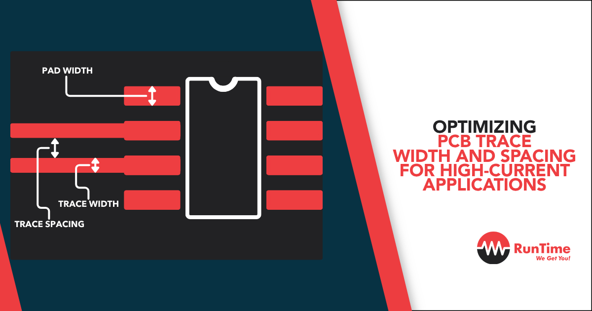
1. Understanding PCB Trace Width and Its Importance
PCB trace width refers to the physical width of the copper pathways on the board that carry electrical current. In high-current applications, trace width becomes a critical parameter due to the need to dissipate heat generated by the current flow. Thin traces may overheat, leading to reduced efficiency or even failure, while excessively wide traces can complicate PCB layout.
Key Considerations for Trace Width:
- Current Carrying Capacity: The higher the current, the wider the trace needs to be.
- Thermal Management: Wider traces spread out heat, helping the PCB maintain a lower operating temperature.
- Voltage Drop: Narrow traces have higher resistance, leading to more voltage drop along the path, which can be detrimental to performance.
A practical starting point for determining trace width is to use established formulas and guidelines based on the current you expect the trace to carry.
2. Standards and Tools for Calculating Trace Width
One of the most commonly used standards for PCB trace width calculation is the IPC-2221 standard, which provides a method for estimating the required trace width based on the amount of current a trace will carry and the allowable temperature rise.
The formula from IPC-2221 for external (outer) layers is as follows:
css
Copy code
I = k × (ΔT^0.44) × W^1.0 × t^0.725
Where:
- I = current (Amps)
- ΔT = allowable temperature rise (°C)
- W = trace width (mils)
- t = copper thickness (oz/ft²)
- k = a constant (0.048 for metric units, 0.024 for imperial units)
For convenience, there are online tools and calculators that can simplify this process. These tools typically allow you to input current, temperature rise, and copper thickness to generate a recommended trace width.
3. Factors Influencing Trace Width in High-Current Applications
While IPC-2221 provides a solid foundation for calculating trace width, several factors unique to high-current applications may influence your final design decisions. These include:
Copper Thickness (Weight)
PCB copper thickness is typically measured in ounces per square foot. Common values are 1 oz, 2 oz, or 3 oz. Thicker copper allows traces to carry more current without excessive heat buildup. In high-current applications, 2 oz or 3 oz copper is often used.
Layer Structure
The position of the trace in the PCB stack-up can affect the amount of current it can safely carry. For example, traces on external layers have better cooling (due to exposure to air), whereas internal traces are more insulated and can retain heat, requiring wider traces.
Operating Environment
Temperature fluctuations, exposure to heat sinks or cooling fans, and proximity to other high-power components can all affect heat dissipation in a PCB. For example, traces in a tightly packed PCB enclosure will require more careful thermal management compared to an open environment.
Trace Shape
Straight traces are preferable for carrying high current. However, in practice, traces may need to curve or have vias connecting different layers. Minimizing sharp corners and avoiding narrow neck-down sections helps reduce resistance and improves current flow.
4. Optimizing Trace Spacing for High-Current PCBs
While trace width ensures the safe conduction of current, trace spacing guarantees that adjacent traces don’t interact with each other in undesired ways, such as through electrical arcing or signal interference.
Electrical Clearance
High current often means high voltage and improper spacing between traces can lead to breakdowns, arcing, or insulation failures. The minimum clearance between traces depends on the voltage applied and the material properties of the PCB dielectric.
A good rule of thumb for electrical clearance is to refer to the IPC-2221 standard, which outlines minimum spacing values based on voltage. For instance:
- 0-100V: Minimum spacing of 0.13mm (5 mils)
- 100-200V: Minimum spacing of 0.25mm (10 mils)
- 200-500V: Minimum spacing of 0.5mm (20 mils)
Thermal Clearance
When adjacent traces carry high current, they can heat up and affect each other’s performance. Wider spacing allows for better heat dissipation and prevents hot spots. It’s recommended to keep critical high-current traces far enough apart to avoid thermal interference.
Electromagnetic Interference (EMI)
High currents can generate significant electromagnetic fields, which may cause interference with nearby signals. Keeping high-current traces separate from sensitive signal traces is essential in minimizing EMI.
5. Techniques for High-Current PCB Design
Beyond simply calculating trace width and spacing, there are several techniques you can use to optimize PCB design for high-current applications.
Using Multiple Layers
One effective way to manage high currents is to use multiple PCB layers for current conduction. By stacking several traces on different layers and connecting them via plated-through vias, the effective trace width increases, allowing the PCB to handle more current.
Wider Pads and Vias
When high current needs to flow between different layers of the PCB, vias must be designed with current capacity in mind. Larger via diameters or even multiple vias can help distribute the current and reduce the risk of overheating or bottlenecking.
Thermal Relief Patterns
For high-current applications, directly connecting copper planes to pads can cause issues during soldering (due to heat sinking). Thermal relief patterns are a solution, ensuring thermal isolation for solder joints while allowing current to flow freely.
Copper Pours and Planes
Using copper pours or large copper areas on internal or external layers can significantly enhance current-carrying capacity. This method allows designers to manage high current without needing excessively wide traces, which can be impractical in some PCB layouts.
Via Stitching for Heat Dissipation
The heat generated in high-current traces can be conducted to other PCB layers using via stitching. This technique places a grid of vias around high-current traces, improving heat transfer to copper planes and enhancing thermal management.
6. Case Study: Designing a High-Current Motor Control PCB
Let’s consider a practical example of designing a PCB for a motor controller, which needs to handle currents of up to 30A. This design requires careful consideration of both trace width and spacing.
Step 1: Estimating Trace Width
Using a 2 oz copper layer, and assuming a permissible temperature rise of 10°C, we use a trace width calculator based on the IPC-2221 standard. For a current of 30A, the required trace width for external layers is calculated to be around 200 mils (5.08mm).
Step 2: Ensuring Adequate Spacing
Given the voltage of the motor control circuit (400V), the minimum trace spacing required is 2mm based on IPC guidelines. However, considering thermal clearance, a larger spacing of 2.5mm is used.
Step 3: Applying Design Techniques
- Copper Pours: Instead of using wide traces, a large copper pour is applied to distribute the current across a broader area.
- Multiple Vias: To connect the copper pours on the top and bottom layers, multiple vias are used to ensure low resistance and adequate heat dissipation.
- Thermal Management: Heat sinks are added to the motor controller’s power section to handle excess heat generated by the high-current traces.
7. Common Challenges in High-Current PCB Design
Heat Management
Excessive heat is a major concern in high-current PCB design. Poor heat dissipation can lead to reduced component lifespan, especially for power components like MOSFETs, diodes, or capacitors. Designers need to incorporate strategies like heat sinks, thermal vias, and copper pours to ensure effective heat management.
Space Constraints
In many designs, space is at a premium, particularly for compact devices like IoT systems or automotive electronics. Fitting wide traces and maintaining proper spacing while keeping the overall size of the PCB manageable can be a challenge. Layer stacking and via stitching can help mitigate this.
Manufacturing Limitations
Not all PCB manufacturers can accommodate very wide traces or high copper weights, especially for boards that use fine-pitch components. It’s important to work closely with your PCB manufacturer to ensure that your design can be produced using their capabilities.
8. Conclusion
Optimizing trace width and spacing for high-current applications is a critical task that impacts both the performance and reliability of a PCB. Following established guidelines, such as those in the IPC-2221 standard, provides a solid foundation for trace width calculations, while thoughtful consideration of thermal management, electrical clearance, and manufacturing constraints ensures that the design will perform well in the field.
By employing advanced techniques like copper pours, multiple vias, and via stitching, engineers can further optimize their designs to handle high currents without excessive heat buildup or signal interference. As always, prototyping and testing are essential to validate the design under real-world conditions.
In high-current applications, proper PCB design isn’t just a matter of following formulas—it’s about balancing performance, reliability, and manufacturability to create a robust solution that meets the demands of modern electronic systems. Whether you’re designing a motor controller or a power supply, understanding how to optimize trace width and spacing is key to success.


