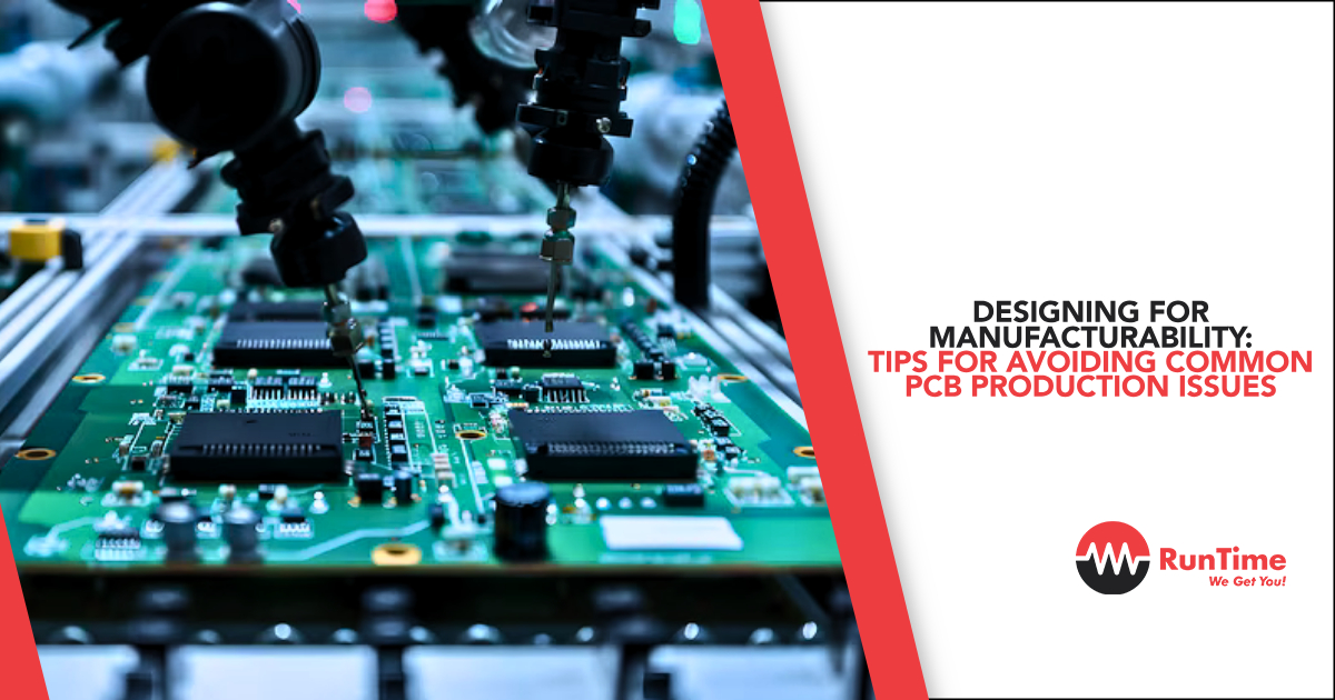
Designing printed circuit boards (PCBs) is an essential part of embedded systems development. While creating the electrical connections for components is one critical part of PCB design, ensuring that the design is manufacturable without defects is equally important. A PCB that’s well-designed for manufacturability (DFM) can save costs, reduce lead time, and prevent issues during production.
This article will explore essential tips for embedded engineers to ensure their PCB designs are optimized for manufacturing. By identifying common PCB production issues and offering practical solutions, we’ll ensure that your boards move smoothly through fabrication and assembly, ultimately reducing errors and improving the overall quality of your product.
1. Understanding Design for Manufacturability (DFM)
Before diving into the tips, it’s essential to define what we mean by “Design for Manufacturability” or DFM. DFM refers to the process of designing a product (in this case, a PCB) in such a way that it is easy and cost-effective to manufacture. For PCBs, this involves understanding the limitations and capabilities of fabrication and assembly processes to avoid errors or expensive redesigns down the line.
DFM involves the following key factors:
- Component placement and routing: Ensuring components are placed in ways that are easy to assemble and test.
- Layer stack-up and via design: Defining the correct number of layers and optimizing via types for manufacturability.
- Clearances: Setting proper spacing between copper traces and components to avoid short circuits or electrical interference.
Now, let’s move into practical tips to avoid common PCB production issues.
2. Keep Design Rules in Check
Every PCB manufacturer will have their own set of design rules that outline the limitations of their process. This includes things like:
- Minimum trace width: The smallest width a copper trace can have.
- Minimum clearance: The smallest distance between two traces, pads, or vias.
- Aspect ratio of vias: The ratio of a via’s hole depth to its diameter.
Ignoring or misunderstanding these rules can lead to rejected designs or production delays. It’s best to consult your manufacturer’s design rule document early in the design process and set up your PCB CAD software to follow these rules. Tools like Design Rule Checking (DRC) in popular PCB design software can help prevent violations.
Tip: Get the Design Rules from Your Manufacturer Early
Some designers wait until the end of the design process to worry about manufacturability. However, getting your manufacturer’s design rules early allows you to incorporate these restrictions into your design from the start. This ensures that you won’t need to rework your design later.
3. Optimize Trace and Space for Signal Integrity
PCB designers often need to balance trace width and spacing with signal integrity. High-frequency signals are particularly sensitive to changes in impedance, parasitic capacitance, and inductance. Issues with trace routing can lead to signal reflections, cross-talk, or noise, ultimately causing the system to fail or malfunction.
To avoid signal integrity problems:
- Match trace lengths: For differential signals, the trace lengths must be matched to prevent timing skew.
- Use ground planes: A continuous ground plane provides a solid reference and minimizes noise and interference.
- Avoid right-angle traces: Right-angle bends can create impedance discontinuities. Instead, use 45-degree bends or gentle curves.
Tip: Use Impedance Calculators
Many PCB CAD tools include impedance calculators or allow for importing material data from manufacturers. This can help you properly size traces for controlled impedance and ensure the signal integrity of high-speed traces.
4. Avoid Overuse of Vias
Vias are used to connect traces between different layers of a PCB. While essential for routing, vias can introduce potential issues:
- Signal degradation: Vias can cause impedance mismatches and affect signal integrity.
- Manufacturing costs: Each via adds complexity and cost to the board, especially if you’re using microvias or buried/blind vias.
Reducing via count can save manufacturing costs and improve the reliability of your board. Instead of relying heavily on vias, consider:
- Optimizing the layer stack-up: Ensure you have enough routing layers and use each layer efficiently.
- Component placement: Arrange components strategically to minimize the number of traces that need to cross layers.
Tip: Use Via-in-Pad with Caution
While via-in-pad can save space in high-density designs, it introduces challenges in assembly, such as solder voids or paste leakage. If you must use via-in-pad, work closely with your manufacturer to ensure proper via plugging or filling.
5. Ensure Proper Component Footprint Design
Component footprints play a crucial role in both the assembly and performance of the PCB. A poorly designed footprint can lead to issues such as soldering defects, misalignment during assembly, or even component damage.
Key factors to consider when designing component footprints:
- Pad size and shape: Ensure that the pad sizes are appropriate for the component leads and soldering process. Too small, and you risk weak solder joints. Too large, and you may have solder bridging.
- Clearances: Ensure sufficient spacing between component pads to prevent solder shorts or misalignment. Follow the IPC standards for pad and clearance sizes.
- Thermal relief: For components that require a solid ground connection, ensure thermal relief is designed into the pads, especially for surface-mount devices (SMDs) to avoid issues during reflow soldering.
Tip: Use Manufacturer-Provided Footprints
Many component manufacturers provide recommended PCB footprints for their components. Always start with these as a baseline to avoid unnecessary rework or soldering issues during production.
6. Account for Solder Mask Expansion
The solder mask is the protective layer that prevents unintended connections or short circuits on your PCB. If the solder mask is incorrectly applied, you may encounter production defects. A common issue arises when the solder mask is too close to the pads or traces, leading to solder mask slivers that can flake off or create short circuits.
To prevent this:
- Ensure proper mask clearance: Use the manufacturer’s recommended clearance between the solder mask and copper features. This allows for manufacturing tolerances and reduces the risk of solder mask peeling.
- Avoid tiny slivers: Minimize small, narrow sections of solder mask that are prone to flaking off.
Tip: Follow IPC Standards for Solder Mask Design
The IPC (Association Connecting Electronics Industries) standards provide clear guidelines for solder mask expansion and other design rules. Using these guidelines can help you avoid common solder mask-related issues.
7. Minimize Thermal Issues in PCB Layout
Thermal management is a critical factor in embedded systems, especially for designs that involve power electronics or components that generate significant heat. Excessive heat can degrade performance, cause component failure, and even damage the PCB over time.
Here’s how you can manage thermal issues in your PCB design:
- Add thermal vias: Use thermal vias to conduct heat from hot components to inner or bottom layers with larger copper pours.
- Copper pours and heatsinks: Utilize large copper pours under high-power components to dissipate heat. You can also integrate metal heatsinks or use thicker copper layers for better heat conduction.
- Component spacing: Avoid clustering heat-generating components in a small area, as this can create local hotspots.
Tip: Run Thermal Simulations
Many PCB design tools include thermal simulation features, allowing you to model heat dissipation and identify areas that might overheat. Running simulations early in the design process can help avoid costly redesigns or performance issues.
8. Ensure Testability in Your Design
Manufacturers often need to test PCBs during and after assembly to ensure that they are functioning correctly. Poor testability can lead to higher production costs and lower yields, especially if defects aren’t caught until late in the process.
For better testability:
- Add test points: Include dedicated test points for critical signals, power, and ground. This allows for easy access during in-circuit testing (ICT) or functional testing.
- Accessible components: Make sure that critical components are easily accessible for probing during testing or debugging.
- Boundary scan/JTAG: For more complex designs, implementing boundary scan or JTAG functionality can greatly aid in diagnosing manufacturing or assembly issues.
Tip: Design for Automated Test Equipment (ATE)
If your design will undergo automated testing, ensure that your test points are compatible with the equipment used by your manufacturer. Provide ample space for probes and access.
9. Avoid Silkscreen Overlaps and Placement Issues
The silkscreen layer is used to print component outlines, part numbers, and other identifiers on the PCB. While it doesn’t affect the functionality of the board, silkscreen misplacement can cause confusion during assembly and inspection.
To avoid silkscreen issues:
- Keep silkscreen off pads: Ensure that the silkscreen doesn’t overlap with solder pads, as this can interfere with soldering.
- Legibility: Make sure the text is large enough to be readable and uses a contrasting color to stand out from the solder mask.
- Proper placement: Ensure that the silkscreen labels are near the components they refer to, but not too close to cause confusion.
Tip: Use Vector-Based Silkscreen Text
Some manufacturers prefer vector-based text for the silkscreen layer, as it provides better accuracy and clarity during printing. Check with your manufacturer for their preferred format.
10. Plan for Soldering Process Requirements
Different components and PCB designs may require different soldering techniques, such as wave soldering, reflow soldering, or hand soldering. Each technique comes with its own set of requirements, and failing to plan for the specific soldering process can result in defects such as cold solder joints or tombstoning.
- Component selection: Ensure that your components are compatible with the chosen soldering process. Some components are designed for specific reflow profiles and may not withstand wave soldering.
- Thermal balancing: Ensure that components with large ground or power planes have thermal reliefs to prevent uneven heating during soldering.
Tip: Consider Panelization for Smaller Boards
If you’re designing a small PCB, consider panelization. Panelization allows multiple boards to be manufactured and assembled in a single run, improving manufacturing efficiency and reducing costs.
11. Work Closely with Your Manufacturer
Throughout the PCB design process, it’s important to maintain an open line of communication with your manufacturer. They can provide valuable insights into their specific fabrication and assembly processes, helping you avoid potential issues before they arise.
Tip: Request a Design for Manufacturability Review
Many manufacturers offer DFM reviews where they will go over your design and highlight any potential issues with manufacturability. This can be a valuable step before committing to a final design.
Conclusion
Designing a PCB for manufacturability is a crucial part of the embedded engineering process. By following the tips outlined in this article, you can avoid common PCB production issues and ensure a smoother transition from design to manufacturing. Key takeaways include adhering to design rules, optimizing trace and via placement, accounting for thermal management, and ensuring testability.
Ultimately, working closely with your PCB manufacturer and using design software that incorporates DFM checks will help you create high-quality, manufacturable PCBs with fewer production issues. Incorporating DFM principles into your design process not only saves time and money but also improves the reliability and performance of your embedded systems.


