Electromagnetic Interference (EMI) and Electromagnetic Compatibility (EMC) are two critical concerns in modern electronics design. With an increasing number of electronic devices being used in close proximity to one another, the likelihood of interference, signal distortion, and equipment malfunction has risen dramatically. Designing for EMI/EMC compliance is not just an industry standard but a necessity for creating robust, safe, and reliable electronics. For embedded engineers, understanding and implementing EMI/EMC best practices during the design process is essential to ensure that their products meet the required standards and function without issues.
In this article, we’ll explore the fundamentals of EMI/EMC, key design considerations, best practices, and testing techniques to help electronics engineers navigate this complex yet essential domain of product design.
Understanding EMI and EMC
Before diving into the best practices, it’s crucial to understand the distinction between EMI and EMC:
- EMI (Electromagnetic Interference): Refers to the unwanted electromagnetic emissions that can disrupt the operation of electronic devices. EMI can be radiated (emitted through the air) or conducted (emitted through power lines or other conductors).
- EMC (Electromagnetic Compatibility): Refers to the ability of an electronic device to operate within its environment without causing or being susceptible to EMI. In simpler terms, EMC ensures that a device doesn’t interfere with other devices and isn’t affected by EMI from external sources.
Achieving EMC involves both controlling emissions from your product and ensuring that the product has immunity to external electromagnetic influences.
Sources of EMI
Identifying the sources of EMI in a design is the first step in tackling it effectively. EMI can originate from various sources, including:
- Switching Circuits: Fast-switching circuits like pulse-width modulation (PWM) circuits, switching power supplies, and high-frequency clock signals are prime sources of EMI.
- Cabling: Long cables can act as antennas, picking up radiated EMI or emitting noise from conducted EMI.
- Ground Loops: Poor grounding or inconsistent ground planes can create loops where EMI noise can circulate and radiate.
- Electromechanical Components: Motors, relays, solenoids, and transformers can all generate significant electromagnetic noise.
- Poor PCB Layout: A poorly designed PCB with inadequate trace separation, improper grounding, or large loops can be a major source of EMI.
Now that we understand the sources of EMI, let’s look at some key design practices that can help mitigate these effects and ensure compliance with EMC standards.
Best Practices for EMI/EMC Design
- PCB Design and Layout
The layout of the Printed Circuit Board (PCB) plays a critical role in EMI/EMC performance. Here are some specific guidelines to follow:- Minimize Loop Areas: Loop antennas are a major source of radiated EMI. Minimize the loop area by placing components and traces close to each other. For example, place decoupling capacitors as close as possible to the power pins of ICs to minimize the power loop area.
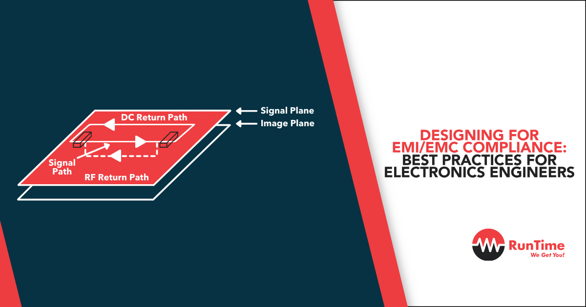
- Use Ground Planes Effectively: A continuous ground plane reduces the risk of EMI by providing a low-impedance return path for high-frequency signals. Avoid cutting the ground plane with traces, as this can lead to ground loops and radiated emissions.
- Signal Trace Routing: Keep high-speed signal traces as short as possible. Routing these signals over the ground plane helps reduce radiated emissions. Differential pairs should be routed close together to cancel out EMI.
- Separate High-Frequency and Low-Frequency Circuits: Isolate high-frequency components from low-frequency ones to prevent EMI coupling. Shielding can also be added for additional protection.
- Controlled Impedance: For high-frequency circuits, controlling the impedance of signal traces is crucial to reduce reflections and radiated noise. Ensure consistent trace widths and appropriate use of termination resistors where necessary.
- Decoupling and Bypassing Capacitors
Decoupling capacitors are essential in controlling EMI. They filter out high-frequency noise from power lines and prevent it from affecting sensitive circuits. Some best practices for capacitor use include:- Use Multiple Capacitors: Employ capacitors with different values (e.g., 0.1 µF, 10 µF) to target a wider range of noise frequencies. Small-value capacitors handle high-frequency noise, while larger capacitors filter out lower-frequency noise.
- Placement: Decoupling capacitors should be placed as close as possible to the power supply pins of ICs. Placing capacitors far from the IC reduces their effectiveness in filtering out noise.
- Shielding
Physical shielding can help contain EMI within a specific area and prevent external noise from affecting the circuit. Key considerations include:- Metal Enclosures: A metal enclosure can act as a Faraday cage, blocking external EMI from penetrating the circuit and preventing internal noise from radiating outward.
- Shielded Cables: Use shielded cables, especially for high-speed or sensitive signals, to prevent them from picking up or emitting EMI.
- Grounding Strategies
Grounding is one of the most important aspects of EMI/EMC design. A poor grounding scheme can lead to ground loops and significant radiated emissions. Some grounding strategies include:- Star Grounding: In star grounding, all circuit grounds are connected to a single point, minimizing ground loops and reducing EMI.
- Chassis Grounding: If your design is enclosed in metal, connecting the circuit ground to the chassis can help dissipate EMI and prevent emissions from radiating.
- Avoid Ground Loops: Ground loops occur when different parts of the circuit are grounded at multiple points, creating a loop where EMI noise can circulate. Star grounding can mitigate this issue.
- Cable Management
Long cables can act as antennas, picking up radiated EMI or emitting noise. Good cable management can reduce these risks:- Twisted-Pair Cables: Twisted-pair cables help reduce EMI by canceling out induced noise between the wires.
- Shielding: Use shielded cables for high-speed data lines or sensitive signals to prevent external EMI from affecting the signal.
- Cable Routing: Route power and signal cables separately. Keep noisy cables (e.g., those carrying switching signals) away from sensitive data lines.
- Use of Ferrite Beads and Chokes
Ferrite beads and chokes are components that help suppress high-frequency noise. They are especially useful in power lines to reduce conducted EMI:- Ferrite Beads: Placed in series with power lines or signal lines, ferrite beads act as high-frequency filters, blocking unwanted noise while allowing the desired signal to pass.
- Common-Mode Chokes: These are used on cables carrying differential signals, such as Ethernet or USB, to filter out common-mode noise without affecting the differential signal.
- Filtering Techniques
Filters can block unwanted high-frequency noise and ensure that only the desired signal passes through. Filtering is especially important in power supply design:- Low-Pass Filters: A combination of resistors and capacitors can create low-pass filters that block high-frequency noise while allowing low-frequency signals to pass.
- EMI Filters: EMI filters can be used in power supply lines to reduce conducted EMI. These filters typically consist of inductors and capacitors that target specific frequency ranges.
EMI/EMC Testing and Certification
After designing with EMI/EMC in mind, it’s essential to test the final product to ensure compliance with the required standards. Here’s an overview of the testing and certification process:
- Pre-Compliance Testing
Before sending your product for formal certification, it’s wise to perform pre-compliance testing in-house. This can help identify EMI issues early and reduce the chances of failing the formal testing phase. Tools such as spectrum analyzers and near-field probes can help identify sources of EMI and evaluate the effectiveness of your design. - EMC Testing Laboratories
For formal certification, your product will need to undergo testing at a certified EMC lab. These labs will test for both radiated and conducted emissions and verify that your product meets regulatory standards (such as FCC, CE, or CISPR). - Test Categories
- Radiated Emissions: Testing for electromagnetic emissions that are radiated through the air.
- Conducted Emissions: Testing for noise conducted through power or signal lines.
- Immunity Testing: Ensuring that your product can withstand external EMI without malfunctioning.
Mitigating Common EMI/EMC Challenges
EMI/EMC compliance can be a tricky process, with challenges often arising late in the design or testing stages. Here are some strategies to address common EMI/EMC challenges:
- Late Detection of EMI: If you discover EMI issues late in the design process, first review the PCB layout for large loops or poorly grounded areas. Adding ferrite beads, shielding, or improving grounding can help reduce emissions.
- Unexpected Test Failures: If your product fails EMC testing, begin by identifying the frequency range of the emissions. This can provide clues about the source of the problem, whether it’s from power supplies, clocks, or high-speed data lines.
- Iterative Testing: EMC compliance often requires multiple iterations of design and testing. Use pre-compliance testing early in the design process to minimize last-minute surprises.
Conclusion
Designing for EMI/EMC compliance is a complex but essential aspect of modern electronics engineering. Embedded engineers who implement best practices early in the design phase can reduce the risk of EMI-related issues, improve product reliability, and ensure compliance with industry standards.
By focusing on PCB layout, grounding strategies, cable management, and effective use of filters and shielding, engineers can create products that operate harmoniously in a crowded electromagnetic environment. Finally, rigorous pre-compliance testing and certification ensure that the product is ready for market without any EMI/EMC setbacks.
For embedded engineers, mastering EMI/EMC best practices is not just about meeting regulatory requirements—it’s about building reliable, high-performance products that work seamlessly in today’s interconnected world.


