Introduction
In the realm of digital design, especially in Field-Programmable Gate Arrays (FPGAs), Clock Domain Crossing (CDC) is a critical concept that embedded engineers need to grasp thoroughly. As modern FPGA designs grow in complexity, the need to manage multiple clock domains effectively becomes increasingly important. Without proper CDC techniques, designs can suffer from metastability, data corruption, and other timing-related issues, leading to unreliable operation.
This article delves into the fundamentals of CDC, the challenges it presents, and the techniques embedded engineers can use to ensure robust and reliable designs.
What is Clock Domain Crossing?
Clock Domain Crossing occurs when a signal passes from one clock domain to another in an FPGA. A clock domain is a section of the design that operates under a specific clock signal. When signals or data are transferred between two different clock domains, which may have different frequencies or phases, timing issues can arise.
The Problem with Multiple Clock Domains
In a synchronous digital system, all signals are typically referenced to a single clock. However, as FPGAs have evolved, it has become common for designs to incorporate multiple clock domains. These domains might operate at different frequencies, have different phases, or even be asynchronous to each other. When signals are transferred from one clock domain to another, there is no guarantee that the receiving domain will sample the signals correctly, leading to potential metastability—a condition where a signal remains in an undefined state for an unpredictable amount of time.
Metastability can cause a chain reaction of failures within an FPGA, propagating incorrect data through the design and leading to unpredictable behavior. To prevent this, engineers must carefully design their systems to manage these clock domain crossings.
Challenges of Clock Domain Crossing
CDC introduces several challenges that must be addressed to ensure the reliability of FPGA designs. The most significant challenges include metastability, data synchronization, and timing closure.
1. Metastability
Metastability is the most critical issue when dealing with CDC. It occurs when a signal from one clock domain is sampled by another clock domain at the wrong time, leading to an undefined output. This can happen when the signal changes state near the sampling edge of the receiving clock.
Metastability can cause a flip-flop to enter an intermediate state, where it does not settle to a logical ‘1’ or ‘0’ within the expected time. This intermediate state can propagate through the design, causing incorrect data or control signals, leading to system failures.
2. Data Synchronization
Data synchronization across clock domains is another major challenge. When transferring data between clock domains, the data must be stable and correctly interpreted by the receiving domain. Inadequate synchronization can result in data corruption, leading to erroneous behavior.
For single-bit signals, the solution might be as simple as a double flip-flop synchronizer. However, for multi-bit data or complex control signals, more sophisticated techniques are required to ensure that the data is correctly aligned and interpreted by the receiving domain.
3. Timing Closure
Timing closure in designs with multiple clock domains is more complex than in single-clock designs. Engineers must ensure that all paths crossing clock domains meet the required timing constraints. This involves careful analysis and implementation of CDC techniques to prevent timing violations that could compromise the design’s functionality.
Techniques for Handling Clock Domain Crossing
To mitigate the risks associated with CDC, several techniques can be employed. These techniques aim to ensure that signals are correctly sampled and data is accurately transferred between clock domains.
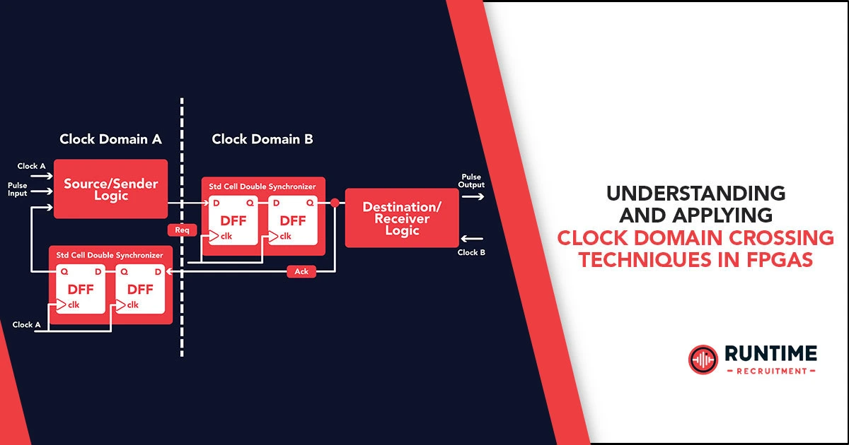
1. Two-Flip-Flop Synchronizer
The two-flip-flop synchronizer is the most basic CDC technique, used primarily for single-bit signals. In this technique, the signal from the source clock domain is passed through two consecutive flip-flops in the destination clock domain. The first flip-flop captures the signal, and the second flip-flop ensures that the signal is stable before it is used in the destination domain.
This technique helps to reduce the probability of metastability, as the signal has a full clock cycle in the destination domain to settle before being used. However, this approach is not suitable for multi-bit data or complex control signals, as it does not ensure that all bits are synchronized simultaneously.
Verilog Example:always @(posedge clk_dest) begin
sync_stage1 <= src_signal;
sync_stage2 <= sync_stage1;
end
In this Verilog example, src_signal is the signal from the source clock domain, and sync_stage2 is the synchronized output in the destination clock domain.
2. Multi-Bit Synchronization Techniques
For multi-bit data, more advanced techniques are required to ensure that all bits are transferred and interpreted correctly. The following are some commonly used techniques:
- Gray Code Encoding: Gray code ensures that only one bit changes between successive values, reducing the risk of data corruption during transfer. This technique is particularly useful for counters or state machines crossing clock domains.
- Handshake Protocols: Handshake protocols involve using control signals to indicate when data is ready to be transferred and when it has been received. This ensures that the data is stable and correctly interpreted by the receiving domain.
- FIFO Buffers: FIFO (First-In, First-Out) buffers are used to safely transfer data between clock domains with different frequencies. The FIFO is designed to handle different clock domains for reading and writing operations, ensuring that data is not lost or corrupted during transfer.
3. Asynchronous FIFO
An asynchronous FIFO is a specialized memory structure designed to handle data transfers between clock domains operating at different frequencies. The FIFO has separate read and write pointers, each driven by a different clock domain. The write pointer operates in the source clock domain, while the read pointer operates in the destination clock domain.
The key challenge in designing an asynchronous FIFO is ensuring that the read and write pointers are correctly interpreted by both clock domains. This is typically achieved by using Gray code for the pointers and synchronizing them across the clock domains.
Verilog Example:module async_fifo(
input wire clk_wr,
input wire clk_rd,
input wire rst_n,
input wire wr_en,
input wire rd_en,
input wire [DATA_WIDTH-1:0] wr_data,
output reg [DATA_WIDTH-1:0] rd_data,
output reg fifo_empty,
output reg fifo_full
);
// Implementation details here
In this Verilog example, clk_wr and clk_rd represent the write and read clocks, respectively, while wr_en and rd_en are the enable signals for write and read operations.
4. Metastability Hardened Flip-Flops
In some cases, it may be necessary to use flip-flops that are specifically designed to reduce the likelihood of metastability. These flip-flops are typically characterized by faster setup and hold times, allowing them to recover more quickly from metastable states.
However, it’s important to note that no flip-flop can completely eliminate the risk of metastability; these specialized flip-flops simply reduce the probability of metastability occurring.
Best Practices for CDC in FPGAs
While understanding the techniques for handling CDC is essential, applying these techniques effectively requires careful design and validation. Here are some best practices for managing CDC in FPGA designs:
1. Identify and Document Clock Domains
The first step in managing CDC is to identify all clock domains in your design. Documenting these domains and their relationships (e.g., frequency ratios, phase offsets) is crucial for understanding potential CDC issues and applying appropriate techniques.
2. Use Formal Verification
Formal verification tools can help ensure that CDC paths are correctly handled in your design. These tools can automatically detect CDC paths and verify that appropriate synchronizers or other CDC techniques are in place. This can help catch potential CDC-related issues early in the design process.
3. Apply Constraints in the FPGA Toolchain
FPGA design tools often allow you to specify constraints for CDC paths, such as false paths or multicycle paths. Applying these constraints helps the toolchain understand the timing requirements for CDC paths, improving the accuracy of timing analysis and reducing the likelihood of timing violations.
4. Perform Thorough Simulation
Simulating your design under various conditions, including worst-case scenarios, is essential for validating CDC handling. Ensure that your simulation environment accurately models clock domain interactions and includes metastability effects. Additionally, perform gate-level simulations with realistic timing models to catch any potential CDC-related issues that may not be evident in RTL simulations.
5. Cross Clock Domains Sparingly
While multiple clock domains are sometimes unavoidable, it’s generally best to minimize the number of CDCs in your design. Fewer CDCs mean fewer opportunities for metastability and other timing-related issues, simplifying the design and validation process.
6. Understand the Trade-offs
Different CDC techniques have different trade-offs in terms of latency, area, and complexity. For example, a two-flip-flop synchronizer is simple and efficient but introduces a delay of two clock cycles. An asynchronous FIFO, on the other hand, can handle larger data transfers and clock domain frequency differences but consumes more resources and adds latency. Understand these trade-offs when choosing CDC techniques for your design.
7. Consider Power Consumption
CDC techniques can impact power consumption, especially in designs with high-frequency clock domains. For example, an asynchronous FIFO can introduce additional switching activity, leading to increased dynamic power consumption. Consider power implications when designing for CDC, particularly in low-power applications.
Real-World Applications and Case Studies
To bring these concepts to life, let’s consider some real-world applications and case studies where CDC techniques have been crucial in FPGA designs.
Case Study 1: Video Processing System
In a video processing system implemented on an FPGA, different modules might operate at different clock frequencies. For example, a video capture module might run at a high frequency to process incoming data quickly, while a display module operates at a lower frequency to match the refresh rate of the display device.
In this scenario, CDC techniques such as asynchronous FIFOs are used to transfer video frames between the capture and display modules. The FIFO ensures that data is safely transferred without loss or corruption, despite the frequency differences between the clock domains.
Case Study 2: Multi-Core Processor Design
In a multi-core processor design on an FPGA, each core might operate in its own clock domain, with a shared memory system operating in yet another clock domain. The challenge here is to ensure that data coherency is maintained when cores access the shared memory.
CDC techniques such as handshake protocols and synchronization mechanisms are used to manage the transfer of data between the cores and the memory system. This ensures that data is correctly synchronized across all clock domains, preventing issues such as data corruption or race conditions.
Conclusion
Clock Domain Crossing is a complex yet essential aspect of modern FPGA design. Understanding the challenges and techniques associated with CDC is crucial for embedded engineers looking to create reliable and robust systems. By applying the right CDC techniques—whether it’s a simple two-flip-flop synchronizer or a more complex asynchronous FIFO—engineers can mitigate the risks of metastability, data corruption, and timing violations.
Incorporating best practices such as formal verification, thorough simulation, and careful documentation can further enhance the reliability of designs involving multiple clock domains. As FPGAs continue to evolve, mastering CDC will remain a critical skill for embedded engineers, ensuring that their designs perform as intended in increasingly complex and demanding applications.
By understanding and applying the techniques discussed in this article, embedded engineers can confidently tackle the challenges of clock domain crossing, leading to more robust and reliable FPGA designs.


