Electromagnetic interference (EMI) and radio frequency interference (RFI) are two of the most challenging obstacles in high-density printed circuit board (PCB) designs. As the demand for smaller, faster, and more complex electronic devices grows, so does the need for robust strategies to minimize EMI and RFI, which can cause significant disruptions in signal integrity and overall device performance. This article delves into the key principles and techniques that embedded engineers can employ to mitigate these issues in high-density PCB designs.
Understanding EMI and RFI
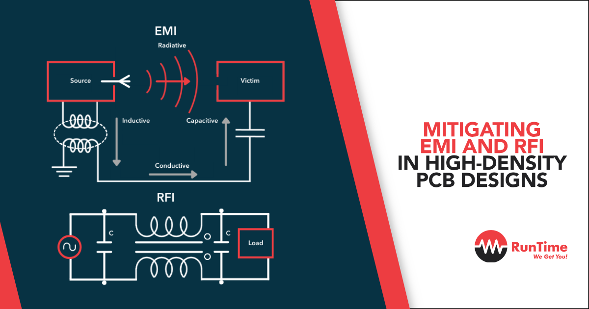
Electromagnetic Interference (EMI) refers to the unwanted noise or interference that affects the normal operation of electronic circuits. It can be caused by both internal and external sources, such as power supply noise, signal crosstalk, or even external electromagnetic fields. EMI can result in degraded performance, data corruption, or even complete system failure.
Radio Frequency Interference (RFI) is a specific type of EMI that occurs within the radio frequency spectrum. RFI can be particularly problematic in wireless communication devices, where it can disrupt signal transmission, leading to data loss and communication failures.
In high-density PCB designs, the proximity of components and traces increases the likelihood of EMI and RFI issues. Therefore, engineers must adopt careful design practices to minimize these effects.
Key Strategies for EMI and RFI Mitigation
1. Layer Stackup Design
The layer stackup is one of the most critical aspects of PCB design for controlling EMI and RFI. A well-planned stackup can provide effective shielding and reduce noise.
- Ground and Power Planes: Incorporate dedicated ground and power planes in the stackup. Placing the ground plane close to the signal layers helps in minimizing the loop area, thereby reducing radiated emissions. The power plane should be adjacent to the ground plane to create a low-inductance path and reduce noise.
- Signal Layer Placement: High-speed signal layers should be placed between two ground planes to provide shielding. This arrangement helps in reducing crosstalk and shielding sensitive signals from external noise sources.
- Controlled Impedance: Ensure that the trace widths and the distance between signal traces and reference planes are controlled to maintain consistent impedance, which is crucial for minimizing signal reflections and radiated emissions.
2. Grounding Techniques
Effective grounding is essential for controlling EMI and RFI. The following techniques can help in achieving a low-impedance ground path:
- Single-Point Grounding: For analog and digital circuits on the same PCB, use single-point grounding to prevent ground loops. Ground loops can act as antennas and radiate noise, so keeping them under control is critical.
- Ground Vias: Use multiple ground vias to connect the ground planes. This reduces the inductance and provides a low-impedance path for return currents, thereby reducing EMI.
- Stitching Vias: For high-frequency designs, consider using stitching vias around the PCB edges and near high-frequency components to create a Faraday cage effect, which helps in containing electromagnetic fields.
3. Trace Routing Best Practices
Proper trace routing is crucial in minimizing EMI and RFI in high-density designs:
- Minimize Loop Areas: The loop area of a current path is directly proportional to the amount of radiated EMI. Therefore, keep the loop areas as small as possible by routing signal and return paths close together. Differential pairs should be routed tightly together to reduce common-mode noise.
- Avoid Sharp Corners: Sharp corners on traces can cause signal reflections and increase EMI. Instead, use curved traces or 45-degree angles for turns.
- Separate High-Speed and Low-Speed Signals: Route high-speed signals away from low-speed signals to prevent noise coupling. If possible, assign different layers for high-speed and low-speed signals.
- Guard Traces and Ground Fills: Place guard traces (ground traces) alongside high-speed signal traces to reduce crosstalk. Ground fills can also be used to provide additional shielding.
4. Decoupling Capacitors
Decoupling capacitors are essential for filtering out noise and providing a stable power supply to the components:
- Placement: Place decoupling capacitors as close as possible to the power pins of ICs. This minimizes the parasitic inductance and effectively filters out high-frequency noise.
- Multiple Capacitor Values: Use a combination of capacitors with different values (e.g., 0.01 µF, 0.1 µF, 1 µF) to cover a wide range of frequencies. The lower value capacitors are effective at filtering high-frequency noise, while the higher value capacitors filter low-frequency noise.
- Bulk Capacitors: In addition to decoupling capacitors, use bulk capacitors (e.g., 10 µF or 100 µF) to maintain a stable power supply, especially during transient events.
5. Shielding
Shielding can be an effective method for containing EMI and RFI:
- Enclosure Shielding: Use metallic enclosures or shielding cans to contain EMI within the PCB and prevent it from radiating to other parts of the device or external environment.
- Trace Shielding: For particularly sensitive traces, consider using a dedicated ground plane directly above or below the trace, effectively sandwiching the trace between two ground planes. This reduces both emissions and susceptibility to external noise.
- Cable Shielding: If the PCB interfaces with external cables, ensure that the cables are shielded and that the shield is properly grounded to the PCB ground.
6. Component Selection
Choosing the right components can have a significant impact on EMI and RFI:
- Low-EMI Components: Opt for components that are specifically designed for low EMI emissions. For example, select power supplies with low noise and filters that meet EMI standards.
- Ferrite Beads: Use ferrite beads on power lines and signal lines to suppress high-frequency noise. They act as low-pass filters, allowing DC signals to pass while attenuating high-frequency noise.
- Differential Signaling: Where possible, use differential signaling instead of single-ended signaling. Differential signaling inherently reduces EMI since the noise is common-mode and cancels out.
7. Filter Design
Filters can be used to block or attenuate unwanted frequencies:
- Low-Pass Filters: Design low-pass filters on power lines to block high-frequency noise. This is particularly important for sensitive analog circuits.
- Common-Mode Chokes: Use common-mode chokes on differential signal lines to filter out common-mode noise without affecting the differential signals.
- EMI Filters: For power entry points, use EMI filters that comply with the relevant standards to block high-frequency noise from entering or exiting the PCB.
8. Simulation and Testing
Simulation and testing are critical steps in ensuring that your design meets EMI and RFI requirements:
- EMI Simulation Tools: Use simulation tools like Ansys HFSS, CST Studio Suite, or Cadence Sigrity to model and predict EMI and RFI behavior in your PCB design. These tools can help identify potential problem areas and allow you to make design adjustments before fabrication.
- Pre-Compliance Testing: Conduct pre-compliance testing during the design phase using a spectrum analyzer and near-field probes. This can help identify EMI hotspots and allow for corrective measures before final testing.
- Compliance Testing: Finally, ensure that your PCB design passes all necessary EMI and RFI compliance tests, such as those required by FCC, CISPR, or MIL-STD-461 standards. Passing these tests is crucial for product certification and market approval.
Case Study: EMI Mitigation in a High-Density IoT Device
To illustrate the application of these principles, let’s consider a case study involving a high-density IoT device. The device in question was a wearable health monitor that required both wireless communication and high-speed data processing, making it susceptible to EMI and RFI.
Challenges:
- High Component Density: The PCB had a high component density with multiple ICs, sensors, and a wireless communication module in a compact form factor.
- Wireless Communication: The presence of a Bluetooth module operating at 2.4 GHz introduced the risk of RFI affecting the nearby analog sensors and microcontroller.
- Power Integrity: The device was battery-powered, with a need for efficient power management to avoid noise affecting the sensitive analog circuits.
Solutions Implemented:
- Layer Stackup Design: A 6-layer stackup was used, with dedicated power and ground planes. The high-speed signals were routed on internal layers between ground planes to minimize EMI.
- Grounding: Multiple ground vias were used to ensure a low-impedance path for return currents. Single-point grounding was implemented to avoid ground loops.
- Decoupling Capacitors: Decoupling capacitors were placed close to the power pins of the ICs, with values ranging from 0.01 µF to 10 µF to cover a wide frequency range.
- Shielding: The Bluetooth module was placed inside a shielding can to prevent RFI from affecting the nearby analog sensors. The enclosure of the device was made of metal, which provided additional shielding.
- Ferrite Beads: Ferrite beads were used on the power lines feeding the analog sensors to suppress high-frequency noise.
- Simulation and Testing: EMI simulation was conducted using Cadence Sigrity to identify potential problem areas. Pre-compliance testing with a spectrum analyzer identified a few hotspots, which were mitigated by adjusting trace routing and adding additional decoupling capacitors.
Results:
The final design passed all required EMI and RFI compliance tests, including those for wireless communication devices. The device was successfully brought to market, with no reported issues related to EMI or RFI.
Conclusion
Mitigating EMI and RFI in high-density PCB designs requires a comprehensive approach that encompasses everything from layer stackup design and grounding techniques to component selection and rigorous testing. By following the strategies outlined in this article, embedded engineers can significantly reduce the risks of EMI and RFI, ensuring that their designs perform reliably in even the most challenging environments.
As electronic devices continue to evolve, the importance of robust EMI and RFI mitigation techniques will only grow. Staying informed about the latest best practices and tools is essential for engineers who want to stay ahead in the competitive field of embedded systems design. With careful planning and execution, it is possible to create high-density PCB designs that meet the highest standards of performance and reliability.


