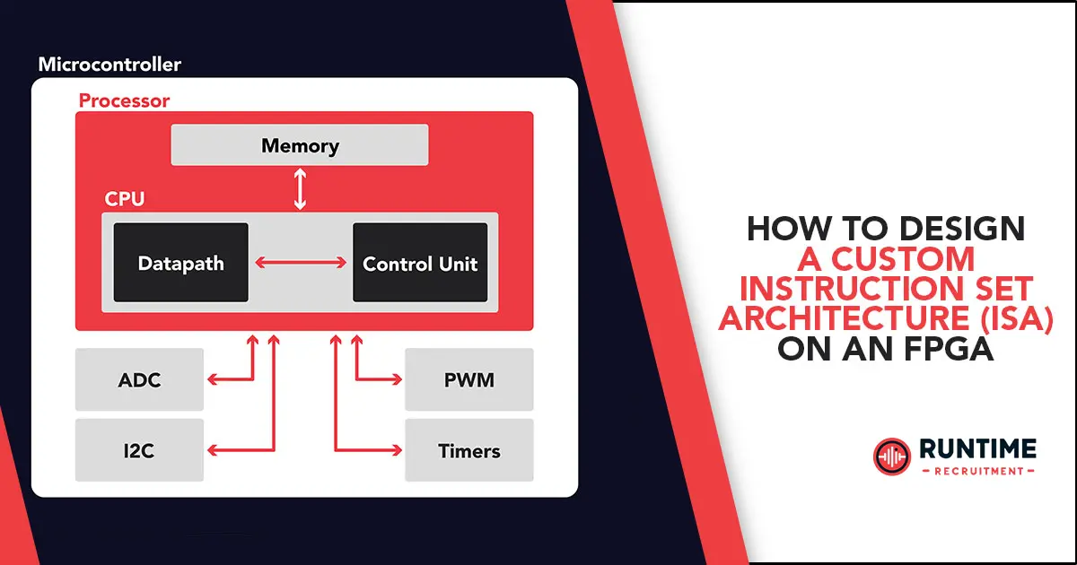
Instruction Set Architectures (ISAs) are the fundamental blueprints defining how software interacts with hardware. Traditionally, these have been rigid, monolithic structures. However, the advent of Field Programmable Gate Arrays (FPGAs) has ushered in an era of unparalleled customization. Now, engineers can craft ISAs tailored to specific computational challenges, unlocking unprecedented performance and efficiency gains.
This article delves into the intricacies of designing a custom ISA on an FPGA. We’ll explore the design process, key considerations, and practical implementation aspects, aiming to equip you with the knowledge to create a processing engine optimized for your unique needs.
Understanding the Basics
Before embarking on ISA design, a solid grasp of foundational concepts is essential.
- ISA Fundamentals: An ISA encapsulates an instruction format, addressing modes, data types, and the instruction set itself. Understanding the nuances of RISC, CISC, and VLIW architectures is crucial.
- FPGA Architecture: FPGAs are composed of configurable logic blocks (CLBs), input/output (I/O) blocks, and memory resources. This flexibility underpins the creation of custom logic, including ISAs.
Defining Your ISA
The cornerstone of any custom ISA is a clear understanding of the target application.
- Identifying the Target Application: Analyze computational requirements meticulously, considering performance and resource constraints.
- Instruction Set Design: Craft an instruction format and encoding that aligns with your application’s needs. Define operation types, addressing modes, and data types carefully.
- Instruction Pipeline and Microarchitecture: Architect a pipeline that optimizes instruction flow, considering hazards and potential bottlenecks. Microarchitectural enhancements can significantly boost performance.
FPGA Implementation
The journey from ISA conception to hardware realization involves critical implementation choices.
- High-Level Synthesis (HLS): HLS tools can streamline the design process by translating high-level descriptions into RTL. However, they have limitations in terms of control and optimization.
- RTL Design: For granular control and maximum performance, manual RTL coding is often necessary. Rigorous verification strategies are paramount.
- Memory Hierarchy Design: Effective utilization of on-chip memory resources (BRAMs, DSP blocks) is pivotal. Careful consideration of memory organization and access patterns is essential.
Verification and Validation
Thorough verification is indispensable to ensure ISA correctness and performance.
- Testbench Development: Create comprehensive testbenches to rigorously evaluate ISA functionality and microarchitecture behavior.
- Simulation and Emulation: Employ software simulation for early-stage validation and hardware emulation for detailed performance analysis.
Optimization and Performance Tuning
Continuous optimization is key to unlocking the full potential of a custom ISA.
- Instruction Scheduling and Code Optimization: Collaborate with compiler engineers to optimize code generation and instruction scheduling.
- Hardware-Software Co-Design: Explore synergies between software and hardware to enhance overall system performance.
Case Studies and Real-World Applications
Real-world examples illuminate the power of custom ISAs.
- Diverse Applications: Explore successful ISA implementations across domains like image processing, signal processing, and machine learning.
- Performance and Efficiency: Compare custom ISA performance against general-purpose processors, highlighting trade-offs between performance, area, and power.
Conclusion
Designing a custom ISA on an FPGA is a challenging yet rewarding endeavor. By following a structured approach and considering the intricacies of ISA design, FPGA architecture, and verification, you can create processing engines tailored to your specific computational challenges. Remember, the journey involves careful planning, iterative refinement, and a deep understanding of your target application.


