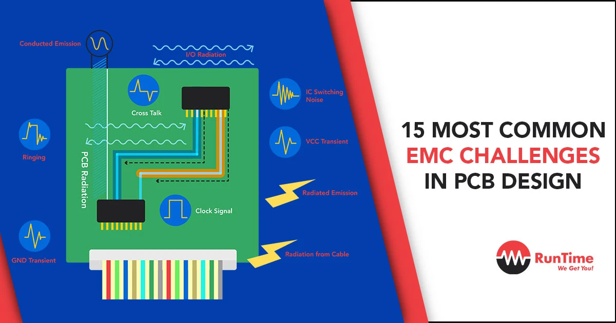
Electromagnetic compatibility (EMC) is a pivotal concern in PCB design, ensuring that a device operates as intended in its electromagnetic environment without introducing intolerable electromagnetic disturbances. Addressing EMC challenges is not just about compliance; it’s a fundamental aspect of product quality and reliability. In this article, let’s discuss the most common EMC challenges in PCB design, offering insights into each issue and suggesting practical solutions.
1. Managing Board Stack-Up Configurations
The stack-up configuration is the foundation of PCB design, impacting signal integrity, power integrity, and EMC performance. A well-designed stack-up can minimize electromagnetic interference (EMI) by optimizing layer arrangement for signal and return planes, reducing loop areas, and enhancing overall board shielding. Designers must carefully consider the number of layers, material properties, and placement of planes to ensure EMC compliance.
2. Controlling Parasitic Elements
Parasitic capacitance and inductance are unintended side effects of component placement and trace routing, which can lead to signal distortion, ringing, and reduced circuit performance. Minimizing these parasitic elements involves careful layout design, including minimizing trace lengths, optimizing component placement, and using differential signaling when appropriate.
3. Ensuring Proper Return Paths
Ensuring a low-impedance path for signal returns is crucial for maintaining signal integrity and reducing EMI. Current follows the path of least impedance, so providing a direct return path close to the signal trace can significantly reduce loop areas and the associated EMI. This is particularly important for high-speed signals, where the return path can dramatically affect performance.
4. Establishing Solid Ground Connections
A robust and continuous ground plane is essential for EMC performance, serving as a reference point for signals and a return path for current. Breaks or gaps in the ground plane can lead to ground loops, increasing EMI. Designers should ensure that ground planes are as uninterrupted as possible and use multiple vias for ground connections to reduce impedance.
5. Utilizing Stitching Vias Effectively
Stitching vias can be used to connect multiple ground planes across different layers, reducing the ground plane impedance and mitigating EMI. They are particularly useful in high-frequency designs where the wavelength of the signals is comparable to the dimensions of the PCB, helping to prevent the formation of unwanted antennas.
6. Mitigating Crosstalk
Crosstalk is the unwanted coupling of signals between adjacent traces or layers, which can lead to signal integrity issues. Mitigating crosstalk involves careful trace routing, maintaining adequate spacing between traces, using ground planes to shield traces, and arranging traces perpendicularly on adjacent layers.
7. Implementing ESD Protection Strategies
Electrostatic discharge (ESD) can damage sensitive components and degrade PCB performance. Implementing ESD protection involves designing in protective components, such as TVS diodes, and ensuring proper grounding and shielding practices to dissipate ESD energy safely away from sensitive circuits.
8. Placing Decoupling Capacitors Correctly
Decoupling capacitors are used to stabilize power supply voltages by providing a local energy reservoir for ICs. Proper placement of these capacitors—ideally as close as possible to the power pins of the ICs they are meant to support—is critical for minimizing impedance and ensuring effective power distribution.
9. Avoiding Placing Traces Too Close to Board Edges
Traces placed too close to the edges of the PCB can act as unintentional antennas, radiating EMI. Maintaining a safe distance between the traces and the board edges, typically at least a few millimeters, can help minimize this risk.
10. Maintaining Appropriate Differential Impedance Levels
Differential signaling can improve signal integrity and reduce EMI by canceling out common-mode noise. Maintaining the correct differential impedance is essential for this cancellation to be effective, requiring precise control over trace width, spacing, and the PCB substrate’s dielectric properties.
11. Signal Integrity Issues
Signal integrity challenges, including reflections, ringing, and attenuation, can degrade performance and contribute to EMI. Addressing these issues involves proper trace termination, impedance matching, and the use of series or parallel termination where appropriate.
12. Power Integrity Problems
Power integrity concerns the ability of the PCB to deliver stable and clean power to all components. Issues such as voltage drops, power rail noise, and switching noise can be mitigated through careful power plane design, the use of bypass and decoupling capacitors, and minimizing impedance in power distribution networks.
13. Thermal Management
The heat generated by components can lead to performance degradation and reliability issues. Effective thermal management, including the use of thermal vias, heat sinks, and careful component placement, is essential for maintaining optimal operating temperatures and ensuring long-term reliability.
14. RF Interference
Radio Frequency Interference (RFI) can be both a cause and a consequence of EMC issues. Mitigating RFI involves shielding sensitive components, filtering inputs and outputs, and designing for specific frequency bands to avoid interference with or from other devices.
15. Harmonics and Filtering
Harmonic frequencies generated by switching circuits can interfere with the operation of other components. Implementing filtering strategies, such as using low-pass filters to remove high-frequency harmonics, is crucial for maintaining signal integrity and compliance with EMC standards.
Wrapping Up
Addressing the common EMC challenges in PCB design requires a comprehensive understanding of electromagnetic principles and a meticulous approach to design and layout. By considering these challenges early in the design process and applying best practices, designers can significantly improve the EMC performance of their products, ensuring compliance with standards and enhancing overall device reliability and quality. The convergence of innovative materials, advanced simulation tools, and iterative design processes is empowering designers to tackle these challenges more effectively than ever before.
Hire the Best Engineers with RunTime Recruitment
If you’re searching for highly skilled engineers worldwide, our expert team of engineers-turned-recruiters is here to help you. We offer in-depth knowledge of technical recruiting in the engineering industry to make the sourcing process much easier for you.
On the other hand, if you’re an engineer looking for new opportunities, RunTime Recruitment’s job site is the perfect place to find job vacancies.


