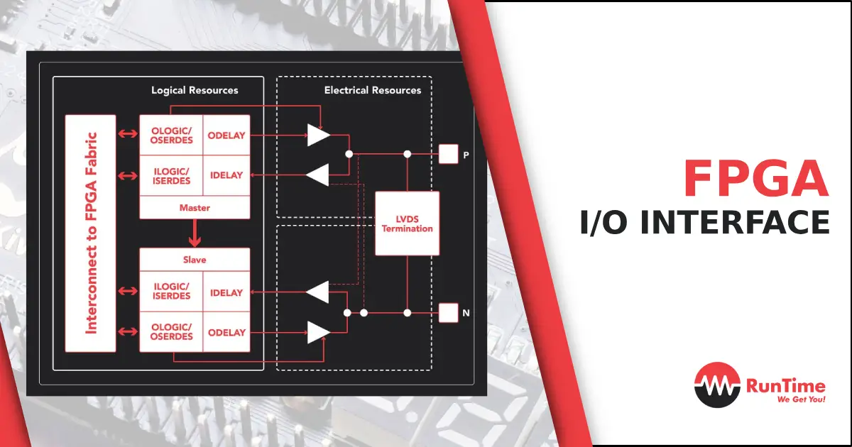
Selecting the appropriate FPGA I/O interface is a pivotal step in designing a system with optimal performance, efficiency, and success. This guide will walk you through the process of choosing the right FPGA I/O interface for your specific application by considering key factors and conducting a comparative analysis of SERDES, LVDS, and GPIO interfaces.
Step 1: Define Application Requirements
Before diving into specific interfaces, clearly define your application requirements. Consider factors such as data rate, power constraints, and environmental conditions. Understanding these key parameters will guide your decision-making process.
Step 2: Comparative Analysis of Interfaces
SERDES (Serializer/Deserializer)
- Ideal for High-Speed Data Transfer: SERDES is well-suited for applications requiring high-speed data transfer. Evaluate if your system demands high-speed communication and if SERDES aligns with your data rate requirements.
LVDS (Low Voltage Differential Signaling)
- High-Speed with Low Power Consumption: LVDS provides high-speed communication with low power consumption and robust noise immunity. Assess whether your application requires these features and if LVDS is a suitable fit.
GPIO (General-Purpose Input/Output)
- Flexibility and Versatility: GPIO offers flexibility and versatility, allowing customization to meet specific application requirements. Consider GPIO if your system demands adaptability and a customized I/O configuration.
Step 3: Comparative Assessment
Compare the advantages and disadvantages of each interface based on your application requirements. Consider factors such as data rate, power consumption, noise immunity, and customization options. This analysis will help you pinpoint the most suitable interface for your project.
Step 4: Evaluate FPGA Device Capabilities
Understand the capabilities and limitations of the FPGA device you intend to use. Each FPGA device has unique features that may impact the compatibility and performance of different I/O interfaces. Ensure that the chosen interface aligns with the capabilities of your selected FPGA device.
Step 5: Thorough Testing and Validation
Once you’ve narrowed down your options, conduct thorough testing and validation to ensure the selected interface meets the performance criteria. Consider real-world conditions, potential variations, and any specific challenges posed by your application.
Step 6: Iterate and Optimize
If necessary, be prepared to iterate and optimize your choice based on testing results. Fine-tune configurations and parameters to achieve the best possible performance for your specific application.
Step 7: Documentation and Future Considerations
Document your decision-making process, including the rationale behind selecting a particular interface. This documentation will be valuable for future reference and can aid in troubleshooting or system upgrades.
Conclusion
By following these steps and conducting a comprehensive analysis, you can confidently choose the right FPGA I/O interface that aligns with your application’s requirements, leading to a more efficient and reliable FPGA system.
Hire the Best Engineers with RunTime Recruitment
If you’re searching for highly skilled engineers worldwide, our expert team of engineers-turned-recruiters is here to help you. We offer in-depth knowledge of technical recruiting in the engineering industry to make the sourcing process much easier for you.
On the other hand, if you’re an engineer looking for new opportunities, RunTime Recruitment’s job site is the perfect place to find job vacancies.


