
Strategies for Preventing Conductive Anodic Filament (CAF) Growth in Ultra-Dense Circuit Boards
22 October 2026 · Lance Harvie
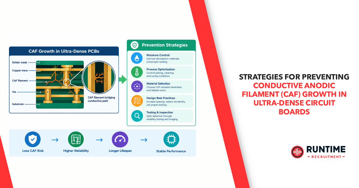
As embedded systems evolve toward higher performance, smaller form factors, and denser component integration, printed circuit board (PCB) architecture has undergone a radical transformation. High-Density Interconnect (HDI) technologies, fine-pitch ball grid arrays (BGAs), microvias, and multilayer stacks with tight clearances are now standard requirements for modern automotive, aerospace, industrial, and high-performance computing applications.
However, this relentless pursuit of miniaturization introduces severe reliability challenges. Among the most insidious silent killers of ultra-dense hardware is Conductive Anodic Filament (CAF) growth.
CAF is an electrochemical failure mechanism that creates internal short circuits within a PCB, often manifesting long after a device has been deployed in the field. For hardware and embedded systems engineers, understanding the root causes of CAF and implementing proactive mitigation strategies at the material, design, and manufacturing stages is paramount to ensuring long-term product reliability.
The Anatomy of CAF: Understanding the Failure Mechanism
Conductive Anodic Filament growth is an electrochemical migration process involving the transport of copper ions along the microscopic interfaces within a PCB’s dielectric material—specifically between the glass reinforcement fibers and the epoxy resin matrix.
For CAF to occur, a combination of four distinct conditions must be present:
An Electric Field (Voltage Bias): A continuous DC potential difference between adjacent conductors, such as plated through-holes (PTHs), inner-layer traces, or microvias.
Moisture: Humidity or ambient moisture that permeates the PCB substrate, acting as an electrolyte.
Ionic Contamination: Residual chemicals from manufacturing, etching, or plating processes that lower the ionic resistance of the moisture path.
A Breakdown of the Glass-Resin Interface: Microscopic debonding or voids between the woven glass fabric and the surrounding resin matrix, creating physical pathways for ion migration.
When these factors converge, an electrochemical reaction takes place. At the anode (positively biased conductor), copper is oxidized into copper ions (Cu2+Cu^{2+}Cu2+ or Cu+Cu^+Cu+). These ions migrate under the electric field through the moisture-filled micro-channels along the glass filaments toward the cathode (negatively biased conductor). Once they reach the cathode, they are reduced back into metallic copper, growing a dendritic filament back toward the anode.
When the filament bridges the gap, it causes a catastrophic insulation resistance drop or a total short circuit, often resulting in intermittent failures that are extremely difficult to diagnose post-deployment.
Why Ultra-Dense and HDI Boards Amplify CAF Vulnerability
Traditional PCBs with wide trace clearances and low operational voltages rarely experienced CAF failures under normal operating conditions. However, ultra-dense circuit boards fundamentally alter the risk profile:
Tighter Spacing: As pitch decreases (e.g., sub-0.5mm BGAs and ultra-fine microvia pitch), the distance between adjacent conductive structures shrinks dramatically. This drastically increases the local electric field gradient (V/mmV/mmV/mm), accelerating the electrochemical migration rate.
Increased Via Density: High-density designs require a massive population of drilled holes, increasing the total surface area of the vulnerable glass-resin interface exposed to drilling-induced mechanical stress.
Higher Operating Voltages in Compact Spaces: Many modern embedded systems combine high-voltage power rails with dense low-voltage digital signal routing on adjacent inner layers, creating high-stress voltage differentials across minimal physical distances.
Thermal Stress: Higher power dissipation leads to localized thermal cycling, which can induce micro-cracks at the glass-resin boundary due to mismatched coefficients of thermal expansion (CTE) between the copper, resin, and glass fibers.
Strategy 1: Material Selection – The Foundation of CAF Immunity
The first and most critical line of defense against CAF is choosing the right base materials. Standard FR-4 laminates, while cost-effective, often lack the interfacial adhesion and moisture resistance required for high-density, high-reliability applications.
Upgrading to Anti-CAF Resin Systems
Modern high-performance laminates feature specialized epoxy resin formulations or modified resin systems (such as filled epoxies, polyphenylene ether (PPO) blends, or cyanate esters) engineered specifically to resist moisture uptake and ionic migration. These materials offer a higher glass transition temperature (TgTgTg) and lower moisture absorption rates, significantly impeding the electrolyte formation necessary for CAF.
Optimizing Glass Cloth Selection
The woven glass fabric is the primary highway for CAF growth. Standard E-glass fabrics have smooth glass filaments held together by silane sizing agents. If this silane bond degrades, microscopic gaps form. Engineers should specify:
Treated or Special-Grade Glass Cloths: Laminates manufactured with proprietary silane treatments that create a chemically robust, moisture-resistant bond between the glass and the resin.
Spread Glass Weaves: Utilizing mechanically or chemically spread glass yarns (such as flat-yarn glass styles). Spread glass eliminates the large resin-rich pockets found at the intersections of traditional woven bundles, shortening potential migration paths and removing the empty spaces where moisture accumulates.
Strategy 2: PCB Design Rules and Geometric Optimization
Even the best materials will fail if the board layout violates basic anti-CAF clearance rules. Layout engineers must transition from designing solely for signal integrity and fabrication yield to designing explicitly for electrochemical reliability.
Hole-to-Hole and Via-to-Trace Spacing
The primary prevention metric in PCB layout is maintaining adequate physical distance between high-potential copper features.
Establish strict design rule check (DRC) parameters that exceed standard minimum manufacturing clearances for nets subjected to continuous DC bias.
Avoid routing high-voltage traces directly parallel to, or immediately adjacent to, unshielded plated through-holes on inner layers.
Anti-Pad and Plane Design
When routing antipads around clearance holes in power and ground planes, ensure that the geometry does not create sharp corners or localized high-field regions. Keep inner-layer clearance distances generous, particularly in environments exposed to high humidity or condensing atmospheres.
Via Configuration Strategies
Staggered vs. Stacked Microvias: While stacked microvias offer superior routing density, they can concentrate mechanical stress along the vertical axis, potentially causing micro-cracking during thermal shock. In highly humid or harsh environments, strategically staggering microvias can disrupt continuous vertical pathways through the dielectric.
Blind and Buried Vias: Utilizing blind and buried vias instead of full-depth mechanical through-holes reduces the total volume of exposed glass-resin interface across the entire board thickness, isolating high-risk zones.
Strategy 3: Manufacturing, Drilling, and Fabrication Controls
The mechanical and chemical processes used during PCB fabrication can inadvertently create the micro-cracks and contamination that initiate CAF. Collaborating closely with fabricators to enforce strict process controls is vital.
Mitigating Drilling-Induced Damage
Mechanical drilling of high-aspect-ratio holes generates immense frictional heat and mechanical shock. If drill bits become dull or feed rates are improperly calibrated, the drill bit can tear the glass filaments rather than cleanly cutting them, causing severe localized delamination and resin fracturing around the barrel of the hole.
Drill Bit Life Management: Fabricators must enforce aggressive tool-change protocols to ensure drill bits never exceed their operational limits.
Optimized Spindle Speeds and Feed Rates: Tailoring drilling parameters to the specific laminate stack-up minimizes thermal and mechanical trauma to the glass bundles.
Chemical Desmear and Plating Optimization
After drilling, the resin smearing the inner-layer copper must be removed using chemical desmear processes. Over-aggressive desmear chemistry can attack the glass-resin interface deeper into the substrate, creating porous channels for moisture ingress. Conversely, incomplete desmear leaves ionic residues and poor copper adhesion. Striking the right balance requires precise bath temperature, chemistry concentrations, and dwell-time controls.
Strategy 4: Post-Fabrication, Assembly, and Environmental Mitigation
Once an ultra-dense PCB is successfully fabricated, protecting it from its operational environment ensures that the internal material boundaries remain dry and uncontaminated.
Ionic Cleanliness Verification
Manufacturing residues, fluxes, and activator salts left on the PCB surface can wick down into micro-vias and drill holes during assembly.
Implement rigorous ionic cleanliness testing (such as Ion Chromatography or ROSE testing) post-assembly.
Ensure ultra-dense boards undergo thorough aqueous cleaning cycles with low surface-tension rinses to remove flux residues from tight-pitch components.
Conformal Coating and Potting
For embedded systems deployed in automotive under-hood, marine, or industrial field environments, external moisture barriers are essential.
Apply high-performance conformal coatings (such as polyurethane, acrylic, or silicone-based formulations) or complete epoxy potting to seal the board against atmospheric humidity ingress.
Ensure coating adhesion is optimized around component leads and edge connectors to prevent capillary moisture penetration.
Testing and Validation Metrics
To verify that an ultra-dense PCB design is truly CAF-resistant before committing to mass production, hardware engineering teams must rely on standardized stress testing protocols:
Surface Insulation Resistance (SIR) Testing: Measuring insulation resistance across closely spaced conductors under elevated temperature and humidity conditions (e.g., 85°C / 85% RH with a continuous DC bias voltage) over hundreds of hours.
Highly Accelerated Stress Testing (HAST): Exposing test coupons to extreme temperature, high pressure, and moisture saturation to rapidly precipitate latent CAF defects and establish the statistical time-to-failure of the laminate stack-up.
Conclusion
As embedded systems push the boundaries of miniaturization, Conductive Anodic Filament growth remains a formidable threat to hardware reliability. Mitigating CAF cannot be treated as an afterthought or left entirely to the PCB fabricator. It requires a holistic, end-to-end strategy—from selecting anti-CAF laminates and spread glass cloths, to enforcing rigorous layout clearance rules, optimizing mechanical drilling parameters, and maintaining stringent environmental cleanliness standards. By designing with electrochemical physics in mind, hardware engineers can build ultra-dense circuit boards that deliver uncompromised reliability in the field.
Looking to hire top-tier embedded engineering talent or find your next career opportunity in hardware design? Connect with RunTime Recruitment.