
Overcoming Ground Loop Distortions in Ultra-Precision Analog Front-End (AFE) Signal Chains
18 November 2026 · Lance Harvie
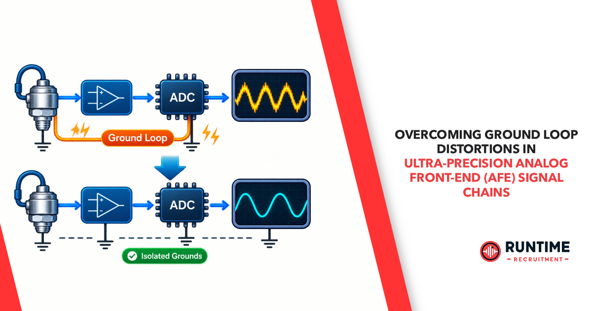
Designing ultra-precision instrumentation — whether for medical diagnostic imaging, high-resolution scientific mass spectrometry, or advanced industrial process automation — presents a relentless, high-stakes war against noise. As semiconductor manufacturers push the boundaries of silicon performance, 24-bit and 32-bit analog-to-digital converters (ADCs) have become industry standards. System architects and embedded hardware engineers now routinely target sub-microvolt noise floors and dynamic ranges exceeding 120 decibels.
Yet, all too often, meticulous schematic capture, component selection, and low-noise power supply design are completely undermined during system integration by a classic, insidious adversary: the ground loop. Ground loops turn a carefully engineered printed circuit board (PCB) into an accidental antenna or a victim of internal voltage drops, stripping away precious bits of resolution and introducing harmonic distortion that digital post-processing can rarely fix.
For embedded engineers building high-performance mixed-signal systems, mastering the root causes and mitigation strategies of ground loop distortions is not optional; it is the definitive factor separating a marketable product from an expensive redesign cycle.
The Anatomy of a Ground Loop in Mixed-Signal Architecture
To defeat ground loops, an embedded engineer must first dismantle the misconception that copper ground planes and traces possess zero impedance. In reality, every trace, via, and cable shield possesses finite resistance and inductive reactance.
A ground loop occurs when two or more points in a circuit that are nominally at the same ground potential are connected via multiple conductive paths, forming a closed loop. In mixed-signal embedded systems, this condition is chronically triggered by the physical coexistence of noisy digital subsystems (microcontrollers, FPGAs, high-speed communication interfaces, and switching power regulators) and ultra-sensitive analog front-ends (AFEs), sensors, and low-level instrumentation amplifiers.
Consider the typical return current path. High-speed digital logic draws sharp, rapid transient current spikes during clock edges and state transitions. These return currents must travel back to the power supply source. If the digital return currents share any portion of the copper ground plane or trace network with the analog return currents, Ohm’s law and Faraday’s law of induction dictate that a voltage drop will develop across that shared section of copper.
When an analog sensor front-end references its local ground to a node that is fluctuating due to digital return currents, that voltage ripple is directly injected into the measurement signal chain. The AFE cannot distinguish between the genuine sensor signal and the self-inflicted ground bounce, resulting in corrupted measurements, erratic system behavior, and severe compliance failures during electromagnetic compatibility (EMC) testing.
Quantifying the Damage: How Ground Loops Degrade Performance
In ultra-precision signal chains, the penalties exacted by ground loops manifest across several key performance metrics:
1. Effective Number of Bits (ENOB) Degradation
The theoretical performance of an ADC is bound by its Signal-to-Noise and Distortion ratio (SINAD), from which the Effective Number of Bits is calculated using a standard logarithmic conversion formula.
When a ground loop injects high-frequency switching noise or low-frequency hum (such as 50 or 60 Hz mains interference via magnetic induction loops) into the analog input or reference pin, the noise floor rises dramatically. A modest increase in the total noise floor obliterates precious bits of resolution. Systems designed for pristine high-resolution performance can easily plummet in effective bit count solely due to poor grounding architecture.
2. Spurious-Free Dynamic Range (SFDR) Contamination
Ground loops often introduce non-linearities and intermodulation distortion. If digital switching noise modulates the analog reference voltage via a shared ground impedance, signal-dependent distortion products appear as spurious peaks across the frequency spectrum, destroying the Spurious-Free Dynamic Range.
3. Thermal and DC Offset Drift
Low-frequency ground currents flowing through resistive copper planes generate localized thermal gradients and static direct-current offsets. In precision DC measurement systems, this manifests as unpredicted drift over temperature and time, ruining factory calibration profiles.
Advanced Hardware and PCB Layout Mitigation Strategies
Mitigating ground loop distortions requires a rigorous hierarchy of design choices, beginning at the schematic level and extending deep into physical layout and system packaging.
The Ground Plane Dilemma: Continuous vs. Split Planes
For decades, a common rule of thumb dictated splitting a PCB strictly into separate analog ground and digital ground planes, tying them together at a single star point underneath the ADC.
While conceptually simple, this approach frequently backfires in modern high-speed designs. When a high-speed digital signal trace crosses the gap between a split plane, its return current is forced to take a massive detour around the split slot to find the single star connection. This enormous loop area acts as an efficient slot antenna, radiating severe electromagnetic interference and creating massive inductive voltage drops.
Modern high-performance mixed-signal design methodology favors a single, continuous, solid ground plane underneath the entire board, coupled with meticulous component placement:
Topography Partitioning: Physically segregate the board layout. Place all noisy digital circuitry, including microcontrollers, memories, and switching converters, on one side of the board, and sensitive analog components, such as sensors, reference ICs, amplifiers, and ADCs, on the opposite side.
Component-Level Grouping: Ensure that the return paths for digital currents never flow underneath or adjacent to sensitive analog signal routing.
The Unified Plane Rule: Allow return currents to choose the path of least inductance directly underneath their corresponding signal traces, maintaining a low-impedance reference across the entire board surface.
Galvanic Isolation
When dealing with remote sensors, industrial machinery, or systems spanning multiple enclosures, ground loops are almost guaranteed due to differing earth ground potentials between locations. In these environments, physical galvanic isolation is mandatory.
Digital Isolators and Optocouplers: Isolate the digital interface side of the AFE using high-speed capacitive or magnetic digital isolators. This breaks the physical DC continuity of the signal path.
Isolated Power Architecture: Isolation is futile if power supplies bridge the gap. Pair digital isolators with isolated DC-DC converter modules or isolated transformer driver ICs to ensure that the primary side, carrying noisy system power, and the secondary side, carrying clean AFE power, share zero common conductive paths.
Fully Differential Signal Conditioning
Single-ended signal chains are exceptionally vulnerable to ground loops because any voltage difference between the source ground and the measurement ground is added directly to the signal.
Transition to fully differential architectures as early in the signal chain as possible.
Utilize high Common-Mode Rejection Ratio instrumentation amplifiers or fully differential amplifiers to drive your ADCs. Because ground loop noise typically appears as a common-mode voltage on both the inverting and non-inverting inputs, a differential architecture cancels out the common-mode interference, preserving signal integrity.
Firmware and Signal Processing Countermeasures
While robust hardware layout and isolation form the primary line of defense, embedded firmware and digital signal processing techniques provide critical layers of defense against residual low-frequency anomalies.
Synchronous Sampling and Chopping
In industrial environments, ground loops frequently pick up line-frequency mains hum via capacitive or inductive coupling.
Chopper-Stabilized Amplifiers: Utilize amplifiers featuring auto-zeroing or chopper stabilization. These architectures modulate input signals to a higher frequency away from direct-current or low-frequency flicker noise and ground loop offsets, and then demodulate them back, effectively cancelling low-frequency error terms.
Mains-Synchronous Sampling: Configure the embedded timer peripherals of your microcontroller to synchronize ADC sampling windows with the local alternating-current mains frequency. By ensuring an integer number of conversion cycles coincide with the mains period, digital moving-average or sinc filters can achieve deep attenuation at line frequencies and their harmonics.
Advanced Digital Filtering Pipelines
Modern sigma-delta ADCs feature programmable built-in digital filters, such as third-order and fourth-order sinc filters. Embedded firmware engineers must carefully configure the output data rate and filter notches to align with known environmental noise profiles. For multi-channel acquisition systems, implementing custom finite impulse response or infinite impulse response notch filters within the microcontroller firmware can target and suppress persistent narrow-band ground loop artifacts that slip past the analog front-end.
Automated Calibration and Auto-Zero Routines
Thermal variations and aging components can exacerbate ground-induced DC offsets over time. Robust embedded software architectures should incorporate routine calibration states. By utilizing internal analog multiplexers to momentarily disconnect the sensor input and short the AFE inputs to a clean local reference, the firmware can measure the residual system offset, including ground-induced errors, and dynamically subtract it from subsequent real-time conversion measurements.
Conclusion
Overcoming ground loop distortions in ultra-precision analog front-end signal chains demands an uncompromising, multidisciplinary approach. Embedded engineers cannot rely on schematic correctness alone; success requires a deep understanding of high-frequency return currents, disciplined PCB floor planning, strategic application of galvanic isolation, and intelligent firmware-level compensation. By treating grounding not as an afterthought, but as the foundational backbone of your mixed-signal architecture, you can preserve the full resolution of your ADCs, achieve rock-solid system stability, and deliver truly world-class instrumentation.
Accelerate Your Engineering Career
Looking to take the next step in your embedded systems or hardware engineering career? Connect with RunTime Recruitment today to explore specialized engineering roles with top-tier technology firms.