
Designing Ruggedized Sensor Interfaces for Sub-Millivolt Precision in Extreme Thermal Cycles
11 November 2026 · Lance Harvie
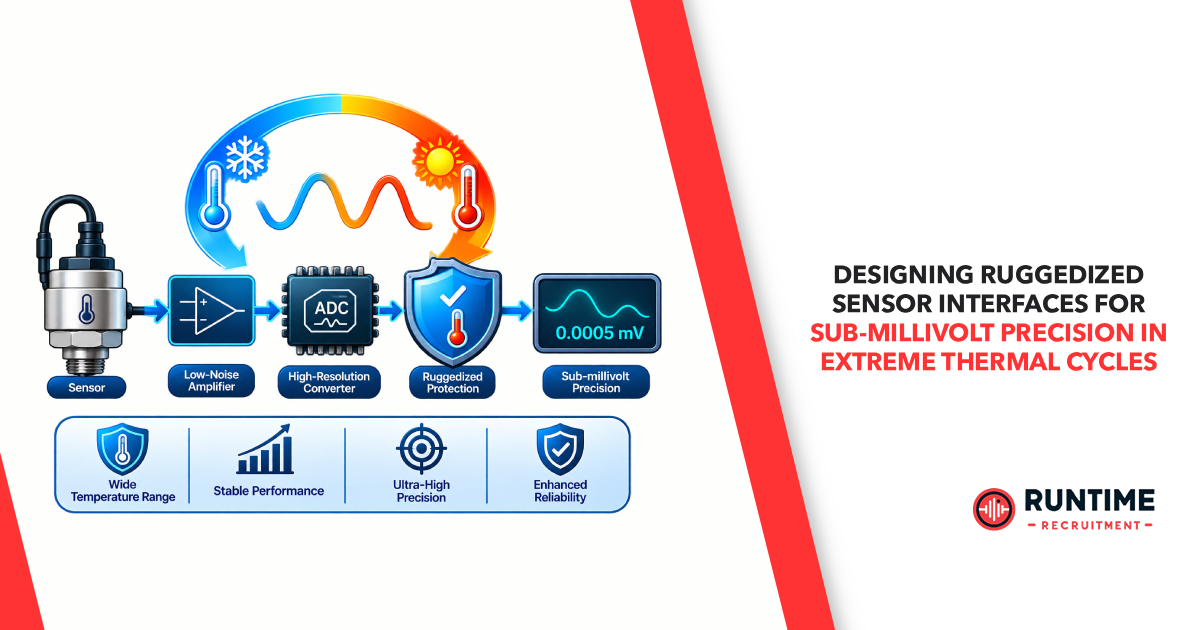
For embedded systems engineers working in aerospace, heavy automotive testing, energy exploration, and industrial automation, bridging the physical world to the digital domain is an exercise in managing harsh compromises. When your system must extract pristine sub-millivolt signals, such as thermocouple outputs, bridge-based strain gauges, or low-side current shunts, while enduring extreme thermal cycles ranging from minus fifty-five degrees Celsius to plus one hundred fifty degrees Celsius and occasionally far beyond, standard design rules fall apart.
In these hostile environments, a microvolt is not just a unit of measurement; it is the thin boundary between a valid reading and catastrophic system failure. Thermal expansion, parasitic thermoelectric junctions, and component drift conspire to introduce errors that easily dwarf the actual sensor signal.
Achieving long-term stability and high-precision accuracy under severe thermal stress requires a holistic engineering approach. This spans from low-level semiconductor selection and advanced printed circuit board layout topologies to intelligent firmware compensation routines and specialized mechanical enclosure design.
1. The Enemy Within: Identifying Sources of Thermal Error
When dealing with signals in the microvolt-to-millivolt range, traditional circuit analysis that assumes ideal components breaks down completely. As temperature fluctuates across the system board, several physical phenomena aggressively degrade measurement integrity.
Parasitic Thermocouple Junctions (The Seebeck Effect)
Every junction of dissimilar metals on your printed circuit board acts as a parasitic thermocouple. Standard solder joints connected to copper traces generate thermoelectric voltages ranging from one microvolt per degree Celsius to upwards of forty microvolts per degree Celsius, depending on the alloy pairing, mechanical stress, and oxidation state.
If a temperature gradient exists across your analog front-end layout — say, a ten-degree Celsius difference between the positive and negative input paths of an operational amplifier — you will instantly inject dozens of microvolts of phantom offset error. In a sub-millivolt measurement system, this single oversight can destroy accuracy before the signal even reaches the analog-to-digital converter.
Input Offset Voltage and Bias Current Drift
Active components are profoundly susceptible to temperature shifts. Operational amplifiers and instrumentation amplifiers feature an input offset voltage drift over temperature. While a standard precision operational amplifier might boast an initial input offset voltage of plus or minus ten microvolts, its temperature coefficient could easily add zero point five microvolts per degree Celsius. Over a one-hundred-degree Celsius swing, drift alone contributes fifty microvolts of error.
Furthermore, input bias currents in complementary metal-oxide-semiconductor and bipolar amplifiers change exponentially with temperature. As the input bias current doubles roughly every ten degrees Celsius, it interacts with source impedances, such as high-resistance resistance temperature detectors or unbuffered bridge sensors, creating significant voltage drops across source resistors and driving the signal wildly out of calibration.
Piezoresistive and Mechanical Stress Effects
Extreme thermal cycles cause constant expansion and contraction of printed circuit board substrates, components, and solder joints. Mechanical stress applied directly to semiconductor dice through package encapsulation or printed circuit board warping induces piezoresistive shifts in silicon. This phenomenon, often overlooked by software-centric engineers, means that mechanical strain translates directly into electrical offset drift, making physical layout rigidity as critical as electrical schematic design.
2. Analog Front-End Architecture and Component Selection
To combat these thermal demons, embedded hardware engineers must carefully select active topologies and specialized integrated circuits designed specifically for harsh-environment precision sensing.
Zero-Drift (Chopper-Stabilized) Amplifiers
For direct current or low-frequency sub-millivolt measurements, standard bipolar or junction field-effect transistor amplifiers are rarely sufficient due to flicker noise and severe offset voltage drift. Instead, zero-drift or chopper-stabilized amplifiers are the gold standard.
Chopper amplifiers continuously correct their own input offset voltage by sampling the offset and subtracting it dynamically using internal switching clocks. Modern zero-drift amplifiers feature offset voltage temperature coefficient figures as low as five nanovolts per degree Celsius, virtually eliminating temperature-induced offset drift.
However, embedded designers must remain vigilant because chopper clocks can introduce high-frequency switching noise and charge injection into the signal path. Careful input filtering, localized shielding, and proper layout spacing are mandatory to prevent this switching energy from aliasing into the passband.
High Common-Mode Rejection Ratio and Differential Signaling
Common-mode voltages induced by thermal ground shifts or electromagnetic interference in industrial settings can easily overwhelm weak signals. Utilizing fully differential signal chains feeding into high-precision, low-noise analog-to-digital converters, such as twenty-four-bit delta-sigma converters, ensures high Common-Mode Rejection Ratio.
When selecting analog-to-digital converters for extreme thermal environments, pay close attention to the internal voltage reference. An external, buried-zener voltage reference with an ultra-low temperature coefficient of three parts per million per degree Celsius or less is almost always superior to integrated bandgap references, which tend to degrade significantly at the outer edges of industrial and automotive temperature ranges.
3. Printed Circuit Board Layout Strategies for Microvolt Integrity
Even the best chopper amplifier will fail if the printed circuit board layout permits thermal gradients or parasitic noise coupling. Layout practices for ruggedized, high-precision interfaces require strict adherence to symmetry and thermal equalization.
Thermal Symmetry and Layout Footprints
The cardinal rule of layout for sub-millivolt precision is absolute thermal symmetry. If a thermal gradient exists across the board, it must affect both the inverting and non-inverting signal paths identically.
Route differential traces close together and in parallel, sharing the exact same thermal environment.
Keep feedback resistors, input protection diodes, and decoupling capacitors symmetrically placed.
Avoid placing high-power components, such as voltage regulators, power metal-oxide-semiconductor field-effect transistors, or communication transceivers, anywhere near the sensitive analog front-end. Establish a dedicated quiet zone or analog island for the sensor interface.
Minimizing Dissimilar Metal Interfaces
To mitigate thermoelectric errors, route signals exclusively through high-grade copper traces and minimize unnecessary transition vias. Ensure that component packaging uses consistent lead frames where possible. Avoid putting dissimilar metal finishes, such as gold-plated pads mating directly with tin-lead component leads without an intermediate barrier, in the direct differential signal path if severe thermal transients are expected.
Substrate and Material Selection
Standard glass-epoxy substrates have a glass transition temperature around one hundred thirty degrees Celsius to one hundred seventy degrees Celsius. If your operating profile pushes near or past these limits, standard material begins to soften, shifting its dielectric constant and placing immense mechanical shear stress on copper plating and vias.
For continuous high-temperature exposure of one hundred twenty-five degrees Celsius or higher, specify high glass transition temperature materials exceeding one hundred eighty degrees Celsius or polyimide-based substrates.
In extreme aerospace or downhole applications, low-temperature co-fired ceramic or thick-film ceramic substrates offer superior thermal expansion matching to silicon and near-zero moisture absorption, drastically cutting down long-term drift.
4. Mechanical Ruggedization, Encapsulation, and Thermal Management
An electronics module that survives electrically on the bench can still fail in the field if mechanical and environmental stressors compromise the hardware packaging.
Conformal Coating, Potting, and Moisture Seeding
In extreme thermal cycles, condensation and humidity pose severe threats. Moisture ingress combined with ionic contamination creates electrochemical migration and leakage currents that completely invalidate sub-millivolt measurements.
Apply high-performance silicone or urethane conformal coatings, or vacuum-pot the analog front-end in specialized thermally stable epoxies.
Crucial Caveat: Potting compounds shrink and expand with temperature. Ensure the compound coefficient of thermal expansion closely matches the printed circuit board components; otherwise, thermal cycling will tear passive components right off the pads or snap delicate wire bonds inside integrated circuit packages.
Thermal Isolation Enclosures
In environments like jet engines or industrial kilns, active cooling is impossible. Instead, engineers must implement thermal lagging and strategic heat sinking. Designing mechanical sub-enclosures with air gaps, thermal barriers such as titanium or ceramic standoffs, and phase-change thermal interface materials protects the sensitive sensor interface from direct thermal shock, slowing down the rate of temperature change over time and allowing internal firmware compensation algorithms to track shifts smoothly.
5. Firmware and Digital Calibration Techniques
Hardware alone cannot achieve absolute perfection across a two-hundred-degree Celsius span. Modern embedded systems rely heavily on firmware-driven calibration and compensation layers to eliminate residual thermal artifacts.
Multi-Point Calibration and Polynomial Modeling
During production test, sub-millivolt sensor modules should be placed in a precision environmental chamber and subjected to a full thermal sweep across various nodes such as minus forty degrees Celsius, zero degrees Celsius, plus twenty-five degrees Celsius, plus eighty-five degrees Celsius, and plus one hundred twenty-five degrees Celsius.
Record sensor output errors at each temperature node using a high-precision onboard temperature sensor placed directly adjacent to the analog front-end.
Generate multi-order polynomial coefficients or lookup tables stored in non-volatile flash memory, such as electronically erasable programmable read-only memory or ferroelectric random-access memory.
During runtime, the firmware reads the local ambient temperature of the front-end, dynamically computes the expected thermal offset and gain error, and applies real-time correction factors to the raw digital converter counts before processing. This ensures that nonlinear thermal variations are smoothed out accurately across the entire operational envelope without hardware redesigns.
Advanced Digital Filtering and Oversampling
Thermal noise increases with absolute temperature and source resistance. To maintain high effective resolution in extreme heat, firmware engineers must leverage aggressive oversampling and digital filtering techniques, such as cascading finite impulse response and moving-average filters or specialized filters native to delta-sigma converters. This trades off a fraction of response bandwidth for a drastically cleaner, noise-resistant measurement output.
Summary Table: Key Design Considerations for Extreme Thermal Environments

Conclusion
Designing ruggedized sensor interfaces capable of resolving sub-millivolt signals through extreme thermal cycles is a multidisciplinary challenge. It demands absolute discipline across hardware architecture, material selection, meticulous printed circuit board routing, and sophisticated firmware calibration. By treating temperature not as an afterthought, but as a primary system variable, embedded engineers can build robust, mission-critical instrumentation that thrives where ordinary electronics fail.
Looking to scale your engineering team with top-tier talent specialized in ruggedized hardware design and embedded firmware? Connect with RunTime Recruitment today to find the technical experts who can bring reliability to your most demanding mission-critical projects.