
Overcoming Transient Response Lag in LDO Regulators for Dynamic Processor Cores
20 October 2026 · Lance Harvie
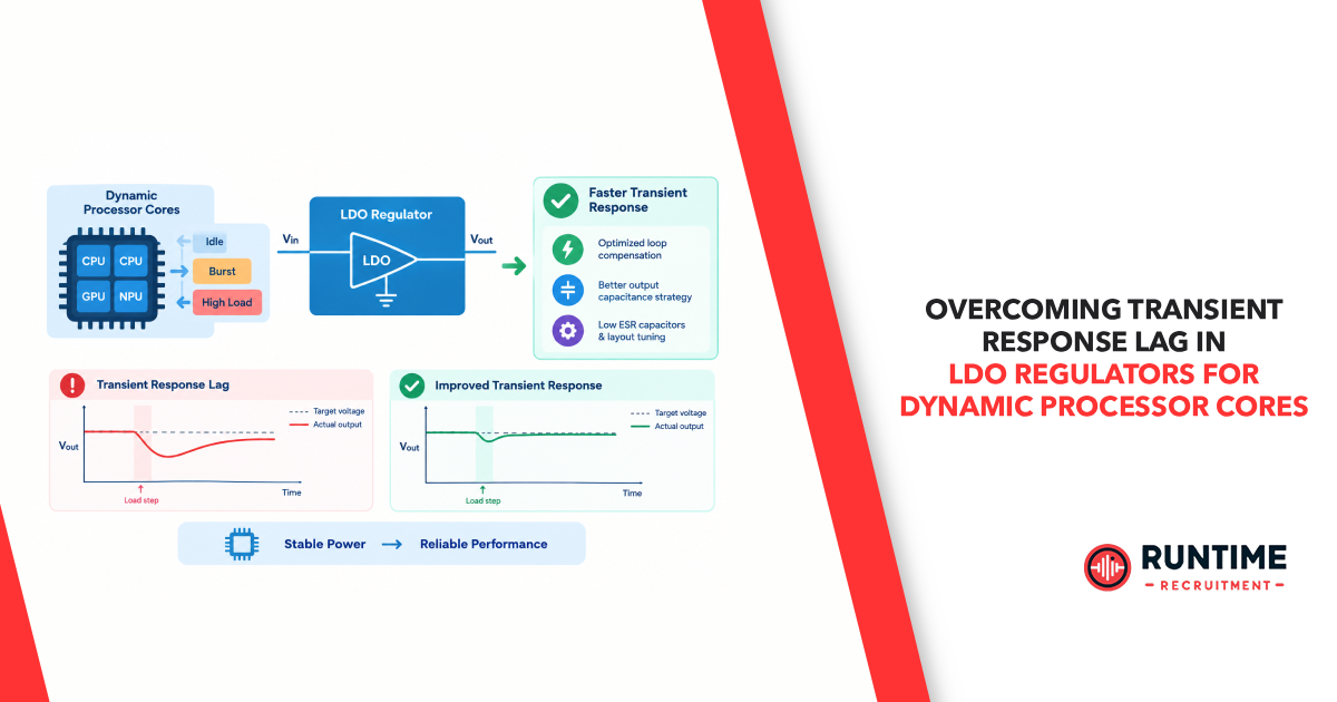
Modern embedded systems are marvels of computational efficiency. Whether powering edge-artificial intelligence accelerators, automotive domain controllers, or high-performance industrial IoT nodes, today's system-on-chips (SoCs) rely heavily on advanced Dynamic Voltage and Frequency Scaling (DVFS). By instantly scaling core voltages and clock frequencies down during idle periods and ramping them up during high-throughput execution, modern processor cores squeeze every microamp of efficiency out of their tight thermal and electrical power budgets.
However, this relentless push toward performance and energy optimization introduces a formidable bottleneck right at the power delivery network (PDN): transient response lag. When a multi-core processor transitions from a low-power deep sleep state to a high-performance active execution state in a matter of nanoseconds, its current demand can jump from a few milliamps to several amps almost instantaneously.
Low-Dropout (LDO) linear regulators are ubiquitous in point-of-load (PoL) regulation due to their low output noise, minimal component count, and spatial efficiency. Yet, traditional LDO architectures frequently struggle to maintain a stable output voltage during these aggressive load steps. The resulting voltage sag can breach the processor's minimum operating voltage threshold, triggering catastrophic logic errors, system crashes, or hard faults.
For embedded hardware engineers, understanding the root causes of LDO transient response lag and mastering modern mitigation strategies—ranging from advanced loop compensation and fast-transient detectors to digital LDO topologies—is critical for building robust, reliable power management systems.
The Anatomy of Transient Response Lag in LDOs
To understand why LDO regulators lag during dynamic load changes, one must examine the internal feedback loop. An LDO maintains a stable output voltage using a negative feedback loop consisting of a reference voltage source, an error amplifier, a pass element (typically a power PMOS or NMOS transistor), and a resistive feedback network.
When a sudden load current step occurs, the sequence of events unfolds through three distinct phases:
Initial Capacitor Discharge: The instantaneous demand for current cannot be met immediately by the regulator's internal loop. Instead, the output capacitor supplies the excess current. Because of its finite capacitance alongside its parasitic Equivalent Series Resistance (ESR) and Equivalent Series Inductance (ESL), the output voltage drops sharply. This initial voltage spike or sag is governed by the immediate capacitive discharge rate and resistive drops across the ESR.
Error Amplifier Propagation Delay: As the output voltage sags, the feedback network transmits this error to the inverting input of the error amplifier. The amplifier must compare this drop against the precision reference voltage and produce an amplified error signal to drive the gate of the pass element. This process is strictly bounded by the amplifier's slew rate, quiescent current, and unity-gain crossover frequency.
Pass Element Charging: The gate capacitance of a large power pass transistor is substantial. Sinking or sourcing enough current to rapidly change the gate voltage introduces a distinct time delay before the pass element can deliver the required load current to the output rail.
This chain of events introduces a fundamental time lag between the occurrence of the load step and the corrective action of the regulator. While this lag might only last for a few microseconds, modern high-performance processor cores can execute millions of clock cycles in that tight window, making transient response lag a severe operational hazard.
System-Level Impacts on Advanced Processor Cores
The consequences of LDO transient response lag extend far beyond a simple dip observed on an oscilloscope screen. In sub-nanometer semiconductor processes operating at core voltages scaling down toward 0.6V to 0.8V, static and dynamic noise margins are remarkably tight.
Voltage Undershoot and Logic Corruptions
When a processor core wakes up from a low-power retention state, the sudden current surge causes an instantaneous voltage sag. If the sag exceeds the static IR drop and dynamic noise budget defined by the silicon vendor, the supply voltage drops below the minimum operational threshold. This leads directly to setup time violations in digital logic paths, corrupted register states, and silent data corruption or immediate kernel panics.
Voltage Overshoot and Oxide Stress
Conversely, when a processor core abruptly transitions from full activity back to a low-power state, the LDO loop, which was previously dumping high current into the load, cannot throttle back instantaneously. The excess energy stored in the control loop and pass transistor rushes into the output capacitor, causing a sharp voltage overshoot. This transient spike can stress gate oxides, violate maximum absolute ratings, or trigger over-voltage protection mechanisms on sensitive digital blocks.
Relying solely on large bulk decoupling capacitors on the printed circuit board (PCB) is no longer a viable silver bullet. At high frequencies, PCB trace inductance forms a severe impedance barrier that isolates remote capacitors from the processor die, forcing the local point-of-load regulator to bear the brunt of the transient response burden.
Advanced Circuit Design Mitigation Techniques
To combat transient response lag, modern LDO architectures integrate sophisticated circuit enhancements designed to bypass traditional analog bandwidth limitations.
Fast-Loop Architectures and Transient Enhancements
Many high-performance LDOs incorporate auxiliary fast-detection circuits operating in parallel with the main error amplifier. These transient detectors monitor the output rail directly via high-speed, low-power comparators. If an abrupt voltage sag or overshoot is detected, the transient enhancement circuit injects or sinks a burst of current directly into the gate of the pass element. This dramatically speeds up its response time without requiring the entire primary feedback loop to operate at an excessively high quiescent current during steady-state conditions.
NMOS vs. PMOS Pass Elements
The choice of pass transistor plays a pivotal role in high-speed transient performance.
PMOS Pass Elements: Traditional LDOs often use PMOS pass elements because they can achieve true low-dropout performance without requiring a higher secondary supply rail for the gate drive. However, PMOS transistors present high input gate capacitance and high output impedance nodes.
NMOS Pass Elements: Modern high-speed LDOs increasingly adopt NMOS pass elements powered by an auxiliary charge pump or secondary high-voltage rail. An NMOS follower configuration provides a much lower output impedance and faster transient tracking, though it demands careful management of gate-drive overhead and minimum input-to-output voltage differentials.
Digital LDO Topologies (D-LDOs)
As core supply voltages scale downward, traditional analog error amplifiers face severe limitations due to reduced intrinsic gain and limited voltage headroom. This has catalyzed the rise of Digital LDOs (D-LDOs).
A D-LDO replaces the traditional analog error amplifier with a flash analog-to-digital converter (ADC) or a time-to-digital converter (TDC). The digitized error signal drives a high-speed digital controller (such as a barrel shifter or up-down counter) that dynamically switches discrete slices of a massive multi-finger transistor array. By eliminating analog compensation poles and utilizing open-loop or predictive digital tracking, D-LDOs can achieve sub-nanosecond response times tailored explicitly for the erratic load profiles of dynamic processor cores.
PCB Layout, Decoupling Strategies, and Co-Design
Even the most advanced monolithic LDO IC will fail to perform if the surrounding hardware implementation introduces parasitic bottlenecks. Embedded engineers must treat power integrity (PI) and physical layout as tightly coupled co-design elements.
Minimizing Loop Inductance: The physical loop area formed by the LDO output pin, the local decoupling capacitors, and the processor power bumps must be kept to an absolute minimum. Every millimeter of trace adds parasitic inductance (Ldi/dt), which directly opposes fast current delivery.
Capacitor Selection and Dielectric Behavior: Multi-layer ceramic capacitors (MLCCs) featuring low ESR and ESL (such as X5R or X7R dielectrics) should be placed as close as possible to the processor power pins. Engineers must also account for DC bias effects, where high-density ceramic capacitors lose a significant portion of their effective capacitance when subjected to a steady DC voltage bias. Combining bulk capacitors for low-frequency charge storage with high-frequency ceramic arrays ensures a flat target impedance profile across a broad frequency spectrum.
Thermal and Ground Management: High transient currents create localized thermal gradients and ground bounce. Solid ground planes and wide, low-impedance power planes are mandatory to prevent reference ground shifts from corrupting the LDO's precision feedback network.
Conclusion
Addressing transient response lag in LDO regulators is one of the defining challenges in contemporary embedded power management. As processor cores become faster, more granular in their power states, and increasingly sensitive to voltage variations, traditional linear regulator design paradigms are no longer sufficient.
By combining an intimate understanding of feedback loop dynamics, implementing advanced fast-loop and digital LDO topologies, and rigorously optimizing PCB-level power integrity, embedded engineers can conquer transient lag. Mastering these techniques ensures that high-performance dynamic processor cores operate reliably, efficiently, and without fear of voltage-induced crashes.
Looking to accelerate your career or scale your engineering team? Connect with RunTime Recruitment to find top-tier embedded systems talent and exciting opportunities in hardware design.