
Mitigating Degradation and Drift in High-Precision Strain Gauge Analog Interface Circuitry
29 October 2026 · Lance Harvie
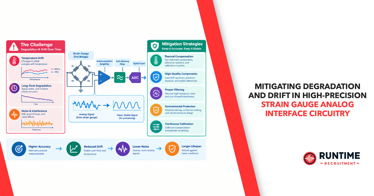
High-precision measurement systems relying on foil resistance strain gauges operate in notoriously hostile environments. From cryogenic wind tunnels and aerospace structural test stands to heavy industrial press floors and high-frequency tactile robotics, these systems are tasked with resolving microvolt-level signals in the presence of severe thermal fluctuations, electromagnetic interference, and mechanical stress.
In these demanding applications, drift and degradation represent the primary failure modes of analog front-end accuracy. Over extended operational lifespans and wide thermal profiles, unmitigated zero-point drift and sensitivity drift erode calibration integrity. This degradation leads to false structural fatigue forecasts, inaccurate load-cell weighings, and catastrophic failures in safety-critical instrumentation.
Designing robust, long-term stable strain gauge interface circuitry requires a rigorous understanding of the physical and electrical mechanisms driving degradation. Embedded hardware and firmware engineers must adopt a holistic approach—spanning bridge excitation, active component selection, circuit-level compensation, and firmware-driven calibration algorithms.
1. The Anatomy of Drift: Root Causes in Strain Gauge AFEs
To effectively mitigate drift, an engineer must first dissect its origins. In a typical Wheatstone bridge configuration coupled with an analog front-end, error sources can be categorized into thermal coefficients, active semiconductor aging, thermoelectric phenomena, and mechanical instabilities.
Thermal Coefficient of Resistance and Gauge Factor
Foil strain gauges are constructed from resistive alloys—such as constantan or karma—bonded to a carrier backing. Two primary thermal coefficients dictate their baseline behavior:
Thermal Coefficient of Resistance: The change in unstrained gauge resistance as a function of temperature.
Temperature Coefficient of Gauge Factor: The change in the strain sensitivity with temperature.
Even when using self-temperature-compensated gauges matched to the thermal expansion coefficient of the structural test material, residual thermal mismatches introduce parasitic resistance shifts that masquerade as mechanical strain.
Active Component and Reference Drift
The analog circuitry conditioning the bridge output is equally susceptible to thermal and temporal degradation:
Voltage Reference Drift: The excitation voltage source sets the scale factor of the bridge output. If the reference voltage drifts by even a few parts per million per degree Celsius, the measurement error scales directly with the excitation level.
Operational Amplifier Offset Drift: Input offset voltage and input bias currents of the conditioning instrumentation amplifier vary with temperature and age. Over a wide industrial operating range, uncompensated offset drift can easily consume a significant fraction of a high-resolution analog-to-digital converter error budget.
Thermoelectric EMFs (The Seebeck Effect)
In high-precision direct current measurement systems, dissimilar metal junctions—formed where copper printed circuit board traces meet component lead frames, solder joints, and connector pins—act as parasitic thermocouples. When a thermal gradient exists across the printed circuit board, these junctions generate Seebeck voltages on the order of microvolts per degree Celsius. Because strain gauge outputs are themselves in the microvolt regime, parasitic thermoelectric EMFs introduce severe low-frequency zero drift that cannot be distinguished from true bridge signals via standard filtering.
Mechanical Creep and Adhesive Degradation
Long-term mechanical stability depends heavily on the bonding adhesive and substrate. Under sustained high loads, elevated temperatures, or humidity ingress, polymer adhesives can experience micro-creep. This mechanical relaxation alters the baseline stress transfer between the specimen and the resistive foil, resulting in permanent zero-shift over months or years of field operation.
2. Bridge Excitation and Interconnection Topologies
The choice of bridge excitation and cabling topology dictates how immune the front-end will be to external environmental variables.
Constant Voltage vs. Constant Current Excitation
Most standard instrumentation designs employ a fixed voltage excitation, such as five volts or ten volts. However, because the resistance of the strain gauge elements and copper lead wires varies with temperature, a constant voltage across the bridge results in an excitation current that fluctuates inversely with temperature.
Alternatively, constant current excitation forces a stable current through the bridge network. While this eliminates sensitivity errors related to bridge resistance thermal variations, it places stringent demands on the stability and noise performance of the current source itself. Furthermore, any change in lead wire resistance directly alters the current distribution if not managed properly through specialized connection schemes.
Kelvin Sensing (4-Wire and 6-Wire Topologies)
In remote measurement applications where the strain gauge is located meters away from the analog front-end, lead wire resistance introduces severe voltage drops and thermal sensitivity.
2-Wire Configurations: Unusable for high precision, as the resistance of the copper leads adds directly to the bridge arms and varies with ambient cable temperature.
4-Wire Configurations: Separates the excitation lines from the measurement lines, though lead resistance in the excitation path still drops total voltage across the bridge.
6-Wire (Kelvin Sensing) Configurations: The gold standard for precision installations. Two dedicated sense lines are routed directly from the excitation pads of the load cell back to the excitation regulation loop or reference inputs. The front-end measures the actual potential difference across the bridge terminals, dynamically compensating for voltage drops and thermal fluctuations in the long umbilical cables.
3. Selecting and Designing the Analog Front-End (AFE)
Architectural selection of the analog front-end sets the upper bound on system performance. Hardware engineers must balance noise, input impedance, common-mode rejection, and drift characteristics.
Traditional Instrumentation Amplifiers (In-Amps)
Traditional three-op-amp instrumentation amplifiers offer exceptionally high input impedance and high common-mode rejection ratio performance. However, standard bipolar or complementary metal-oxide-semiconductor instrumentation amplifiers suffer from significant flicker noise at low frequencies and pronounced direct current offset drift over temperature.
Zero-Drift (Chopper-Stabilized) Amplifiers
To conquer flicker noise and thermal offset drift, modern high-precision designs utilize zero-drift or auto-zero architectures. These amplifiers employ internal switching networks and auxiliary nulling loops to dynamically cancel out input offset voltages and low-frequency noise continuously.
Design Caveat: Engineers must account for switching ripple and charge injection spikes originating from the internal chopping clocks. Proper differential resistance-capacitance filtering at the amplifier output is essential to prevent intermodulation distortion and aliasing into the signal band.
Delta-Sigma Analog-to-Digital Converters with Integrated PGAs
For direct digitization, high-resolution 24-bit delta-sigma converters integrate low-noise programmable gain amplifiers and internal digital filters. These devices offer excellent noise performance, internal calibration modes including offset and gain self-calibration, and flexible digital filtering that notches out line frequency interference. When paired with low-drift external voltage references, these converters form the backbone of modern compact industrial weighing and force-measurement electronics.
4. Advanced Circuit-Level Mitigation Techniques
Beyond component selection, specific circuit topologies can neutralize environmental degradation vectors before they reach the digitization stage.
AC Bridge Excitation
To combat direct current thermoelectric EMFs and amplifier offset drift entirely, hardware designers implement alternating current bridge excitation. Instead of applying a continuous direct current voltage, the bridge is driven by a bipolar square wave or sine wave excitation source.
The analog front-end samples the bridge output synchronously with the excitation polarity, known as synchronous demodulation. Because parasitic thermal EMFs and amplifier offsets remain unmodulated with constant polarity, they are successfully shifted to the switching frequency and filtered out by subsequent low-pass or band-pass filters, leaving only the pure bridge signal to be recovered.
Passive Component Selection and Layout Symmetry
The bridge completion network—if external precision resistors are used—must be constructed using ultra-low thermal coefficient metal-film or bulk metal foil resistors exhibiting minimal resistance tracking variation across temperature ranges. Standard thick-film chip resistors introduce massive thermal errors and resistance drift over time.
Furthermore, printed circuit board layout demands rigorous thermal symmetry. Differential signal traces must be routed with identical lengths and tightly coupled geometries. Placing bridge completion resistors and amplifier input stages in close thermal proximity, away from localized heat sources such as power regulation metal-oxide-semiconductor field-effect transistors or microcontrollers, prevents intra-board thermal gradients from generating differential offset errors.
5. Firmware-Driven Calibration and Thermal Compensation
Hardware alone cannot eliminate all physical drift; firmware intelligence is required to close the loop on long-term stability.
On-Board Thermal Mapping
High-precision systems should incorporate high-accuracy digital temperature sensors or precision resistance temperature detectors placed physically adjacent to the strain gauge rosette and reference circuitry. This provides real-time thermal telemetry synchronized with raw bridge measurements.
Polynomial and Spline Compensation Modeling
During factory environmental chamber testing, systems are subjected to calibrated temperature sweeps and mechanical loads. Firmware engineers utilize this characterization data to construct multi-order polynomial equations or multi-dimensional lookup tables representing the offset and sensitivity behavior across the entire operational temperature envelope.
During active operation, the microcontroller applies dynamic compensation coefficients based on real-time temperature sensor readings, actively subtracting thermal zero and sensitivity shifts from the raw digital output.
Automated Tare and Autozero Routines
To combat long-term mechanical creep and aging-induced baseline drift, firmware should implement intelligent autozero routines. When the system detects a verified unloaded state through motion sensors, command triggers, or specific timeout criteria, it captures a new baseline zero-offset and stores it in non-volatile memory such as electrically erasable programmable read-only memory or ferroelectric random-access memory. This ensures that cumulative mechanical relaxation does not saturate the measurement range over years of field deployment.
6. PCB Layout and Physical Design Best Practices
Precision analog layout is an exercise in discipline. A pristine schematic can be completely compromised by poor physical execution:
Grounding Strategy: Maintain a clean analog ground plane isolated from digital switching noise. Tie analog and digital grounds together at a single, well-defined star point, typically located at the converter ground pin or power entry.
Guard Traces and Shielding: In high-impedance, humid environments, surface leakage currents across printed circuit board solder masks can inject errors into high-gain nodes. Implement driven guard rings surrounding sensitive signal traces, maintained at the same potential as the signal node to eliminate parasitic leakage paths.
Enclosure and Potting: Protect the analog frontend from ambient airflow drafts and rapid thermal transients by utilizing heavy-gauge metal shielding enclosures or thermal potting compounds that increase the thermal mass and time constant of the sensor electronics.
Conclusion
Mitigating degradation and drift in high-precision strain gauge interface circuitry is a multidisciplinary challenge requiring meticulous attention to physical phenomena, component physics, analog front-end architecture, and embedded firmware compensation. By combining Kelvin sensing topologies, zero-drift amplification, alternating current excitation, thermal mapping, and robust printed circuit board layout, embedded engineers can build measurement systems capable of maintaining exceptional stability across extreme operational lifespans.
Connect with RunTime Recruitment
Looking for top-tier embedded engineering talent for your next mission-critical hardware project? Connect with RunTime Recruitment today.