
Addressing Power Integrity Degradation Driven by Fast Transient High-Core Current Demands
21 October 2026 · Lance Harvie
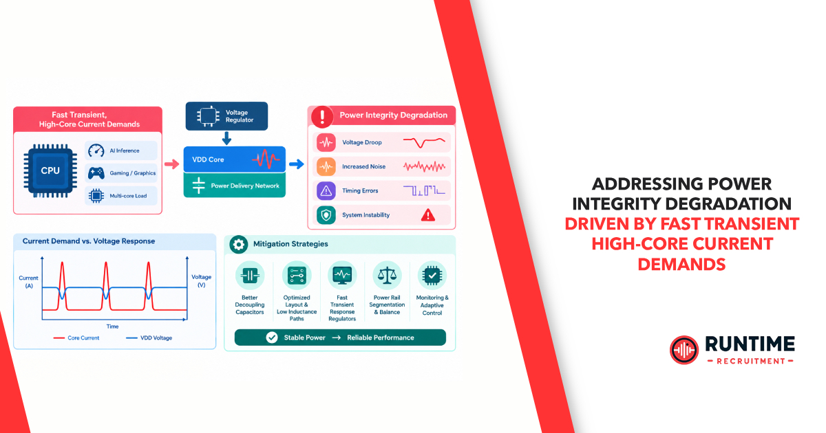
Introduction: The High-Performance Power Crisis
If you are an embedded hardware or systems engineer designing with modern sub-nanometer SoCs, high-density FPGAs, or multi-core application processors, you have likely encountered a terrifying phenomenon: a sudden, catastrophic system crash or silent data corruption triggered not by software bugs, but by a microscopic voltage dip.
As semiconductor process nodes shrink to 3nm and below, operating voltages continue to plummet while core current demands skyrocket. Modern processing units can transition from deep idle states to full computational throttle in mere nanoseconds. This sudden surge in current demand, characterized by aggressive current change rates over time, wreaks havoc on traditional Power Distribution Networks (PDNs). Power integrity degradation is no longer a niche concern reserved for multi-gigabit server board designers; it is an everyday battleground for embedded engineers pushing the boundaries of edge computing, automotive ADCs, and high-speed communication hardware.
When a processor demands dozens or hundreds of amperes of core current within a fraction of a clock cycle, the physical laws governing inductors and conductors push the system to its absolute limits. This article explores the root causes of power integrity degradation under fast transient high-core current conditions, analyzes the frequency-domain mechanics of PDNs, and outlines actionable, hardware-level mitigation strategies to keep your power rails rock-solid.
The Physics of Failure: Anatomy of a Transient Voltage Droop
To understand why power integrity collapses under heavy transient loads, we must look beyond static DC calculations and examine the dynamic realities of transient physics.
When a processor core wakes up or executes a heavy compute vector, its current draw shifts almost instantaneously. Ohm’s law and Faraday's law of induction dictate how the PDN responds. The voltage drop experienced at the IC power pins during a current step is fundamentally governed by three major components:
IR Drop (Resistive Loss): The static voltage loss across the DC resistance of the copper planes, traces, and package interconnects. While straightforward to calculate, high-current rails—such as fractional-volt cores drawing tens or hundreds of amperes—require massive copper volume to keep resistive loss within a strict three to five percent tolerance window.
LC Resonant Voltage Droop: The reactive response of the PDN's inherent inductance and capacitance, which can create localized ringing and resonant voltage valleys across the power network.
Inductive Voltage Drop: The dynamic voltage drop driven by parasitic loop inductance combined with the rapid rate of change of current over time. When current changes instantly, even tiny parasitic inductances generate significant counter-electromotive forces that directly subtract from the supply voltage at the silicon die.
Why the Voltage Regulator Module Can't Save You Fast Enough
A common misconception among junior engineers is that a high-end, multi-phase Voltage Regulator Module (VRM) can instantly compensate for sudden core current spikes. In reality, a VRM is physically separated from the silicon die by centimeters of PCB traces, vias, BGA balls, and package routing.
Because of this physical distance, the loop inductance between the VRM and the load is significant, typically ranging from tens to hundreds of nanohenries. Electrical signals and energy wavefronts propagate at finite speeds, and inductive reactance acts as a massive roadblock to high-frequency current changes.
While a VRM is exceptionally skilled at regulating DC and low-frequency current variations ranging from direct current up to a few hundred kilohertz, it is completely blind and unresponsive to nanosecond-scale transients. When a fast transient hits, the VRM takes microseconds to respond—an eternity in digital logic. During this window, the local circuitry must rely entirely on stored local charge reservoirs. If those reservoirs fail, the supply voltage collapses, timing margins evaporate, and the processor experiences a brownout or hard fault.
Frequency-Domain Engineering and Target Impedance
Achieving robust power integrity requires shifting your perspective from the time domain to the frequency domain. Every PDN must be viewed as a complex impedance network comprising resistance, inductance, and capacitance spanning from DC to several gigahertz.
Managing the Maximum Allowable Impedance Ceiling
The golden rule of power integrity design is maintaining a flat, low PDN impedance profile that stays strictly below a calculated ceiling known as the target impedance. This target threshold is derived directly from the maximum allowed voltage ripple divided by the maximum transient current step your system will ever experience.
For instance, consider a modern low-voltage SoC core operating below a single volt with an allowable ripple budget of three percent and a worst-case transient current step reaching tens of amperes. Maintaining an impedance below a few milliohms across a broad frequency spectrum—from DC to over one gigahertz—is one of the most rigorous challenges in hardware engineering. If your network impedance rises above this threshold at any frequency, a current transient at that specific frequency will trigger excessive voltage ripple and potential system failure.
The Decoupling Hierarchy and Frequency Bands
To cover this vast frequency range, engineers deploy a hierarchical network of components, each owning a specific frequency band:
DC to Low Kilohertz (The VRM Domain): Handled directly by the main switching regulator and bulk output capacitors. The VRM provides the low-frequency energy pool.
Intermediate Frequencies (The Bulk Capacitor Domain): Large electrolytic, tantalum, or high-value ceramic bulk capacitors act as regional charge buffers to handle intermediate load steps.
High Frequencies (The Ceramic Decoupling Domain): Surface-mount multi-layer ceramic capacitors placed meticulously close to the IC package pins provide the high-frequency charge required during rapid switching events.
Ultra-High Frequencies (The Package and On-Die Domain): At these frequencies, external PCB components become entirely inductive due to mounting and equivalent series inductance. Mitigation here relies entirely on the integrated circuit package capacitance and microscopic on-die decoupling capacitors embedded directly into the silicon substrate.
The Danger of Anti-Resonance
A common pitfall when placing multiple decoupling capacitor values in parallel is the creation of anti-resonance peaks. When a larger capacitor transitions from capacitive to inductive behavior at its self-resonant frequency, it can form a parallel resonant tank circuit with a smaller capacitor that is still capacitive.
This parallel resonance creates a massive impedance spike that drastically exceeds your target threshold. If a high-core current transient excites this specific frequency band, the resulting voltage ripple will be severely amplified, causing intermittent system crashes. Mitigating anti-resonance requires carefully blending capacitor values, utilizing controlled equivalent series resistance damping, and minimizing the total number of distinct capacitor values on the rail.
Advanced PCB Layout and Stackup Strategies
You can select the finest low-ESR ceramic capacitors and the most advanced multi-phase VRMs available, but a poor PCB layout will still guarantee power integrity failure. Minimizing loop inductance on high-current rails dictates every millimeter of your board geometry.
Optimizing Power and Ground Planes
The most effective high-frequency decoupling element on a printed circuit board is not a discrete component—it is the inherent distributed capacitance formed by adjacent power and ground plane pairs.
Tight Dielectric Spacing: Choose thin core prepregs for your primary power-ground plane sandwiches. Closer planes dramatically increase inter-plane capacitance and reduce cavity loop inductance.
Solid Planes without Splits: Avoid routing high-speed signal traces or creating split voids directly underneath high-core current areas. Any slot or split in a reference plane forces return currents to take long, circuitous detours, vastly increasing loop area and inductive voltage spikes.
Minimizing Mounting and Via Inductance
The loop inductance of a decoupling capacitor is determined by the total area of the current loop, which includes the capacitor's internal equivalent series inductance, the soldering pads, breakout traces, and the vias connecting to internal planes.
Embrace Via-in-Pad: For high-density BGAs drawing massive core currents, standard dog-bone fanout routing introduces unacceptable trace inductance. Utilizing via-in-pad technology directly beneath or immediately adjacent to decoupling pads cuts breakout trace length to near zero.
Multiple Vias per Pad: Never rely on a single via to connect a decoupling capacitor or power pin to a plane. Use pairs or quads of parallel vias to divide current and reduce total via barrel inductance.
Symmetrical Placement: Place smaller, higher-resonant-frequency capacitors as physically close to the processor power pins as geometry permits. A small capacitor placed too far away is virtually useless at high frequencies due to the added trace loop inductance.
Component Selection & Modern Decoupling Tactics
Selecting components for high-transient rails goes beyond reading nominal capacitance values on a datasheet.
Understanding Capacitor Realities
Real capacitors are far from ideal; they behave as series resistance-inductance-capacitance networks. Below its self-resonant frequency, a capacitor exhibits capacitive reactance. Exactly at its resonant frequency, its impedance bottoms out to equal its equivalent series resistance. Above that frequency, parasitic equivalent series inductance dominates, causing the component to act like an inductor.
To combat high-core current transients:
Prioritize Low ESL Packages: Choose reverse-geometry capacitors, where terminations are on the long side of the chip to shorten current paths, or multi-terminal capacitor arrays to drastically lower parasitic inductance.
Control Dielectric Characteristics: Class 2 ceramic dielectrics offer high volumetric efficiency, but their capacitance changes significantly with applied DC bias voltage. Always consult DC bias derating curves; a nominal capacitor operating under a DC bias may yield only a fraction of its rated capacitance in actual circuit operation.
Simulation, Verification, and Measurement Pitfalls
Verifying power integrity cannot wait until prototype boards return from the assembly line. Modern embedded design workflows demand rigorous pre-layout and post-layout simulation.
Simulation Tools and Methodologies
Frequency Domain Solver: Extract scattering parameters of the entire power distribution network from the voltage regulator output terminals all the way to the integrated circuit package bumps. Plot the impedance profile across frequency to verify that your network impedance stays safely below your target threshold.
Transient Simulation: Model worst-case current step profiles to observe immediate voltage droop and ringing across the die pads.
Measurement Challenges in the Lab
Measuring sub-millivolt high-frequency noise on high-current rails is notoriously difficult. Common mistakes include:
Using Ground Leads: Ground leads on oscilloscope probes act as antennas, picking up massive amounts of electromagnetic interference and creating artificial high-frequency ringing. Always use low-inductance spring-tip ground adapters or coaxial browser probes.
Bandwidth Limitations: Ensure your oscilloscope and probe combination possess adequate bandwidth to capture fast transient dips without attenuation.
Conclusion
Addressing power integrity degradation driven by fast transient high-core current demands requires a holistic, physics-first engineering approach. By understanding the strict limitations of remote voltage regulators, managing frequency-domain impedance thresholds, optimizing PCB stackups and plane geometries, and minimizing mounting inductances, embedded engineers can conquer the challenges of modern high-performance silicon. Power integrity is no longer an afterthought; it is the fundamental foundation upon which reliable, robust embedded hardware is built.
Connect with RunTime Recruitment
Looking to scale your embedded engineering team? Connect with RunTime Recruitment today to find elite hardware and power integrity specialists for your next project.