
Addressing Memory Contention in Multi-Master Bus Architectures Using Hardware Semaphore IP
27 October 2026 · Lance Harvie
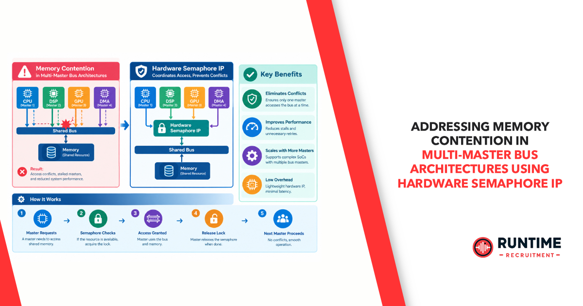
As modern embedded systems evolve from single-core microcontrollers to complex heterogeneous System-on-Chips (SoCs), the architectural demands placed on internal interconnects have shifted dramatically. Today’s high-performance embedded designs frequently feature multi-master bus architectures—combining multi-core application processors, real-time microcontrollers, direct memory access (DMA) controllers, and custom hardware accelerators or FPGA fabric blocks—all contending for shared resources such as off-chip DRAM, internal SRAM scratchpads, and peripheral register banks.
While advanced bus matrices and high-throughput interconnect fabrics like AMBA AXI4 or TileLink do an exceptional job of managing data routing, they do not inherently solve the problem of logical synchronization. When multiple masters attempt to read, modify, and write to the same shared memory locations simultaneously, memory contention devolves into race conditions, data corruption, and catastrophic system instability.
For embedded systems engineers and hardware-software co-designers, mitigating this contention without sacrificing real-time determinism is one of the most persistent challenges in SoC design. While software-based synchronization primitives have traditionally been the default fallback, scaling multi-master systems demands a hardware-native approach: the Hardware Semaphore Intellectual Property (IP) block.
The Anatomy of Bus Contention in Multi-Master Systems
To understand why traditional synchronization breaks down, we must first look at how multi-master bus architectures handle data transactions. In a typical SoC, masters connect to a central bus interconnect or crossbar switch. Arbitration units within the interconnect govern access permissions based on schemes such as round-robin, fixed-priority, or weighted fair-queuing.
However, bus arbitration only dictates who gets access to the physical wires at any given clock cycle; it has zero visibility into the logical intent of the software or hardware transactions. Consider a scenario where Master A (a real-time Cortex-R core) and Master B (an FPGA-based packet processor) both need to update a shared circular buffer located in a shared SRAM bank.
If both masters execute a read-modify-write sequence concurrently, the following failure mode occurs:
Master A reads the head pointer from shared memory (Value = 0x10).
Master B reads the head pointer from shared memory (Value = 0x10).
Master A calculates the new pointer (0x14) and writes it back.
Master B calculates its new pointer (0x18) and writes it back, overwriting Master A’s update entirely.
The physical bus handled both transactions successfully, but the system state is corrupted because there was no atomic exclusion protecting the critical section.
Why Software-Based Synchronization Hits a Wall
Traditionally, embedded engineers rely on software-based synchronization mechanisms to enforce mutual exclusion. These include:
Spinlocks and Mutexes: Utilizing atomic instructions like ARM’s LDREX/STREX (Load-Exclusive / Store-Exclusive) or RISC-V’s LR/SC pairs.
Software Flags: Polling shared memory locations where a core continuously reads a flag until it clears.
While these primitives work well in homogeneous, low-master environments, they introduce severe bottlenecks in complex multi-master architectures:
1. Bus Saturation and Traffic Amplification
When multiple cores or masters are blocked on a software spinlock, they continuously poll the shared memory location. In a system with multiple masters executing millions of polling reads over an AXI interconnect, this generates immense background traffic. The interconnect becomes saturated with atomic read-modify-write requests, starving legitimate data payloads of bandwidth and degrading overall system throughput.
2. Cache Incoherency and Snooping Overhead
In systems where masters feature local data caches, heavy software lock contention triggers continuous cache invalidation cycles (snooping traffic). The cost of maintaining cache coherency across masters while thrashing a lock variable can consume significant dynamic power and introduce unpredictable latency spikes.
3. Priority Inversion and Determinism Failure
In hard real-time embedded systems, predictability is paramount. If a low-priority master holds a software spinlock and is preempted or delayed by bus arbitration, high-priority masters waiting on that lock experience unbounded priority inversion. Software locks offer little to no hardware-enforced determinism regarding who acquires the lock next.
Introducing Hardware Semaphore IP
To eliminate the systemic inefficiencies of software synchronization, modern SoC architectures integrate a dedicated Hardware Semaphore IP block directly into the memory map.
A Hardware Semaphore IP is a centralized, lightweight hardware peripheral designed specifically to manage atomic locks and resource ownership across multiple asynchronous masters. Rather than forcing masters to battle over shared system memory or cache lines, masters interact with a dedicated register bank within the semaphore block via low-latency peripheral buses (such as APB or AXI4-Lite).
Core Architectural Features of Hardware Semaphore IP
Atomic Test-and-Set Registers: Each semaphore channel typically corresponds to a single hardware register. A read operation returning a specific value (e.g., 0) and simultaneously setting the bit ensures true atomic acquisition in a single bus cycle.
Master ID Tagging: Advanced semaphore IPs automatically record the bus ID or master ID of the entity that successfully claimed the semaphore. This provides instant traceability for debugging and error handling.
Hardware Interruption Support: Instead of polling, masters can configure semaphores to trigger an interrupt when a contested lock is released, allowing sleeping cores to wake up only when the resource becomes available.
Timeout and Deadlock Watchdogs: Robust IP designs include programmable timeout counters. If a master crashes or hangs while holding a critical semaphore, the hardware automatically releases the lock after a specified number of clock cycles, preventing permanent system deadlocks.
Architectural Deep Dive: Integrating Hardware Semaphores
Implementing a hardware semaphore block into an FPGA or ASIC design requires careful consideration of the register map, interface protocols, and failure modes.
1. The Register Interface
Typically, a hardware semaphore block exposes an array of semaphore channels mapped to a specific address space. For example, a 32-channel semaphore block might occupy 128 bytes of memory-mapped I/O.
Writing to a specific channel address attempts to acquire the semaphore.
Reading from the channel returns the current owner or status.
Writing a release code (or writing 0) releases the semaphore.
2. Arbitration at the Peripheral Level
Even the semaphore IP itself must handle simultaneous access requests from multiple masters. Because two masters might attempt to write to the exact same semaphore register on the exact same clock edge, the hardware IP internal finite state machine (FSM) must serialize these requests. Using internal priority encoders or round-robin arbiters on the IP input ports guarantees that only one master wins the race condition at the hardware gate level, returning a "success" or "failure" status flag in the response phase of the bus transaction.
3. Integrating with RTOS and Bare-Metal Drivers
On the software side, integrating hardware semaphores involves writing lightweight abstraction layers that replace traditional software spinlocks. For instance, in a FreeRTOS or Bare-Metal environment running on a dual-core SoC:
// Conceptual Hardware Semaphore Acquisition Function
bool hw_semaphore_take(uint8_t channel_id) {
// Attempt atomic acquisition via memory-mapped hardware register
HW_REG_SET(SEMAPHORE_BASE + (channel_id * 4)) = MASTER_ID_CURRENT_CORE;
// Read back to verify if this core successfully secured ownership
if (HW_REG_READ(SEMAPHORE_BASE + (channel_id * 4)) == MASTER_ID_CURRENT_CORE) {
return true; // Acquired successfully
}
return false; // Contended / Failed
}
By offloading the synchronization logic to dedicated hardware gates, the CPU cycles spent waiting are reduced to near-zero, and bus traffic is restricted to a single atomic handshake rather than continuous polling loops.
Real-World Use Cases in Heterogeneous Systems
Hardware semaphore IPs shine brightest in complex architectures where disparate processing units must cooperate without human intervention or OS-level abstraction layers.
Case Study: Dual-Core ARM Cortex-R5 and FPGA Accelerator Co-Processing
Consider an automotive radar processing unit. A dual-core ARM Cortex-R5 processor manages system scheduling and network stacks, while a heavy-duty FFT hardware accelerator synthesized in the FPGA fabric processes raw analog-to-digital converter (ADC) streams. Both units write data into a shared double-buffered ping-pong SRAM structure.
Without hardware semaphores, the Cortex-R5 would need to use complex software mutexes located in the shared SRAM, resulting in cache-snooping overhead and unpredictable interrupt latency for the safety-critical radar pipeline. By placing a Hardware Semaphore IP between the interconnect and the SRAM controllers, the FPGA accelerator instantly locks Buffer A upon completion, signals the ARM core via a hardware interrupt routed through the semaphore block, and switches processing to Buffer B with zero bus contention.
Multi-Core Microcontrollers in Industrial Automation
In industrial motor control applications utilizing quad-core ARM Cortex-M or RISC-V microcontrollers, multiple cores frequently access shared peripherals (such as PWM generation blocks and high-speed ADC sampling registers). Hardware semaphores ensure that control loops executing on different cores never interleave their register configurations, guaranteeing deterministic execution times required for sub-millisecond motion control loops.
Best Practices for Hardware-Software Co-Design
When designing or integrating Hardware Semaphore IP into your next embedded architecture, keep the following engineering best practices in mind:
Map Semaphores to Non-Cachable Memory Regions: Ensure that the memory-mapped address space allocated for the hardware semaphore block is explicitly marked as non-cachable (e.g., Device or Strongly Ordered memory in ARM architectures) in the Memory Protection Unit (MPU) or Page Table Entries. Caching semaphore registers defeats their atomic purpose.
Implement Fallback Timeouts: Never rely solely on infinite-wait loops in production firmware. Configure hardware watchdog timers on critical semaphore channels to recover gracefully from master faults or bus lockups.
Keep Lock Granularity Fine: Rather than using a single global semaphore for an entire memory subsystem, instantiate multi-channel semaphore blocks to allow fine-grained locking per data buffer, peripheral, or memory region, maximizing system concurrency.
Verify with Constrained Random Simulation: During RTL verification, subject the hardware semaphore interconnect to aggressive multi-master constrained random simulation to flush out rare race conditions, deadlock states, and arbitration dead zones.
Conclusion
As embedded systems continue to scale in processing power, core count, and architectural complexity, software-only synchronization is no longer sufficient to handle the realities of memory contention. Bus saturation, cache thrashing, and unpredictable determinism make traditional spinlocks a bottleneck in high-performance designs.
By leveraging dedicated Hardware Semaphore IP, embedded systems engineers can offload atomic synchronization to the hardware layer, ensuring deterministic multi-master coordination, preserving precious bus bandwidth, and unlocking the full potential of heterogeneous SoC architectures.
Looking to connect with top-tier embedded engineering talent or find your next career challenge in advanced hardware-software co-design? Connect with RunTime Recruitment today.