
Dual-Bank Flash Swaps: Preventing Unrecoverable Bricks During Power Interruption Mid-A/B Update
11 August 2026 · Lance Harvie
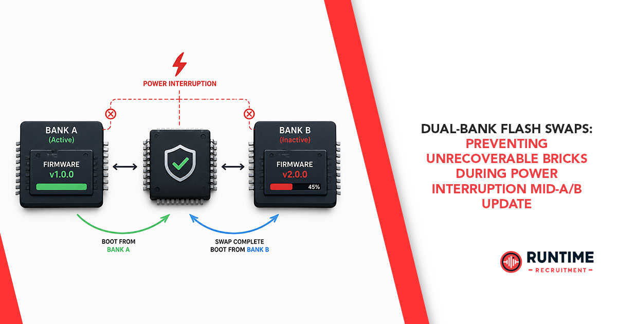
Every embedded engineer has experienced the cold sweat of a potential field failure. Imagine a fleet of remote industrial sensors, automotive ECUs, or medical devices deployed across thousands of customer sites. An Over-The-Air (OTA) firmware update is broadcast across the network. Midway through writing the new binary image into internal flash memory, a power failure occurs—a drained battery, a grid brownout, or an operator accidentally pulling the plug.
If the system relies on a traditional single-bank flash memory architecture, this single event can be catastrophic. The existing application code is partially erased or corrupted, leaving the device stranded in an incomplete bootloader loop or completely unresponsive—a state known as "bricking". Recovering thousands of bricked devices in the field requires expensive manual intervention, physical JTAG re-flashing, or costly RMA returns.
To guarantee fail-safe, zero-downtime updates in mission-critical embedded devices, modern microcontroller (MCU) architectures feature Dual-Bank Flash memory and A/B swap capabilities. In this deep dive, we will examine how dual-bank flash operates, analyze failure vectors during power loss mid-update, and outline a bulletproof architecture to prevent unrecoverable bricks.
Single-Bank vs. Dual-Bank Flash Memory
Before evaluating the bank swap process, we must understand why single-bank updates are inherently fragile.
In traditional single-bank MCUs, the CPU fetches and executes instructions from the same physical flash bank where application code resides. Flash memory technology prevents reading from a bank while an erase or write operation is active on that same bank—a hardware restriction causing CPU stalls or bus lockups. Consequently, in-place updates require a dedicated bootloader executing either from a protected flash sector or copied into SRAM.
During a single-bank update, the bootloader erases the active application sectors and programs new image blocks directly into that space. If power drops mid-write, the application image is permanently corrupted. While a resilient SRAM bootloader might attempt recovery, it relies on immediate power restoration, stable network connectivity, and external storage buffers. If the bootloader itself is corrupted during an update, remote recovery over the wire is impossible.
Dual-Bank flash architectures eliminate this vulnerability by splitting physical internal flash into two independent memory banks: Bank A (Bank 0) and Bank B (Bank 1). Each bank possesses its own dedicated flash controller hardware, decoding logic, and sense amplifiers. This physical separation unlocks two critical capabilities:
Read-While-Write (RWW) / Background Operation (BGO): The CPU executes instructions continuously from Bank A while the integrated flash controller erases or programs pages in Bank B without stalling the system bus.
Hardware Address Aliasing (Bank Swapping): The MCU's system bus decoder can dynamically remap memory addresses. Whichever bank is designated active automatically aliases to logical base address 0x0000_0000 (or 0x0800_0000).
The Anatomy of an A/B Firmware Update Lifecycle
The A/B update paradigm utilizes dual-bank memory to maintain a two-slot operational model. At any given time, one bank operates as the Active Slot (Slot A) running production firmware, while the opposing bank serves as the Inactive Staging Area (Slot B).
A fail-safe A/B update lifecycle follows a five-stage state machine:
Stage 1: Background Payload Streaming
The application runs normally from Bank A. As update packets arrive via cellular, BLE, or CAN bus, a background task streams the binary chunks directly into physical Bank B. Due to Read-While-Write support, normal device operations and user services continue uninterrupted.
Stage 2: Cryptographic & Header Verification
Once the complete binary resides in Bank B, the running application verifies image integrity before touching boot registers. It computes a cryptographic digest (e.g., SHA-256) and verifies an asymmetric digital signature (e.g., ECDSA P-256 or RSA-2048) against a public key anchored in secure bootloader memory or a Hardware Root of Trust. It also checks image metadata, including version numbers and target device IDs.
Stage 3: The Swap Atomic Commit
After successful verification, the firmware updates non-volatile configuration registers—commonly designated as Option Bytes, Flash Control Registers, or Fuse Bits (such as the BFB2 bit in STM32 MCUs or BKSWRST in Microchip SAM E units). Setting this hardware flag instructs the system bus matrix to remap physical Bank B to logical address 0x0000_0000 upon the next system reset.
Stage 4: Hardware Reset & Memory Remap
The application issues a software reset (NVIC_SystemReset()). During power-on reset sequence, the hardware checks the option bytes, swaps memory bank aliases, and vectors CPU execution into the new image in Bank B.
Stage 5: Post-Boot Health Validation
The newly executed firmware in Bank B initializes peripherals and performs internal self-diagnostics. If health checks pass, the application writes a validation flag to persistent metadata storage, confirming the update as permanent.
Threat Modeling Power Loss Across the Update Sequence
To build an unbrickable system, firmware architects must analyze power loss at every millisecond of the update sequence.
+------------------------------------------------+
| Firmware Update Starts |
+----------------------+-----------------------+
|
v
+-------------------------------------------------------+
| Stage 1: Download Image to Bank B |
+-------------------------+----------------------------+
|
[ Power Loss ] –-+--> [ Safe Fallback ]
Boots active Bank A on power restore.
Bank B partial binary re-erased.
|
v
+----------------------------------------------------+
| Stage 2: Integrity & Signature Check |
+------------------------+--------------------------+
|
[ Power Loss ] --+--> [ Safe Fallback ]
Boots active Bank A on power restore.
Option bytes remain untouched.
|
v
+------------------------------------------------------+
| Stage 3: Atomic Option Byte Commit |
+------------------------+----------------------------+
|
[ Power Loss ] --+--> [ Hardware Protected ]
Shadow registers & hardware parity
prevent corrupted option byte state.
|
v
+-----------------------------------------------------+
| Stage 4 & 5: Boot & Health Validation |
+-----------------------+----------------------------+
|
[ Power Loss ] --+--> [ Rollback Triggered ]
or System Crash Hardware Watchdog forces reset;
bootloader reverts option byte to Bank A.
Scenario 1: Interruption During Payload Download (Stage 1)
Risk: Bank B contains incomplete binary garbage.
Recovery: Zero risk. Upon reboot, the hardware reads the original Option Bytes, which still point to Bank A. The MCU executes the existing application code cleanly. Bank B is simply cleared when the update task restarts.
Scenario 2: Interruption During Signature Verification (Stage 2)
Risk: The binary is fully written, but integrity checks were incomplete.
Recovery: Zero risk. Because Option Bytes were never modified, the system reboots into Bank A undisturbed.
Scenario 3: Interruption During Option Byte Commit (Stage 3)
Risk: Power fails while the Flash Controller is writing to the non-volatile bank swap register. Can an incomplete write cause an ambiguous hardware state?
Silicon Safeguards: Microcontroller manufacturers protect this critical window:
Shadow Registers & Double Buffering: Option bytes are loaded into staging shadow registers and committed atomically using specific unlock sequences (e.g., unlocking FLASH_KEYR and FLASH_OPTKEYR).
Complementary Bits & ECC: Swap configurations use complementary bit values (e.g., 0x5A active vs 0xA5 inactive). An interrupted write generates an invalid parity state, forcing the hardware logic to default safely to Bank A.
Immutable ROM Bootloader: If dual-bank fuse configurations become corrupted, internal factory ROM bootloaders intercept execution for low-level recovery.
Scenario 4: Interruption During First Boot & Health Check (Stages 4 & 5)
Risk: Bank B is active, but power fails during peripheral initialization—or the new binary contains a fatal runtime bug (e.g., HardFault or infinite loop) that prevents self-validation.
Recovery: Handled via a Hardware Watchdog + Boot Counter rollback mechanism.
Engineering Implementation Strategies for Fail-Safe Swaps
Hardware capabilities must be paired with disciplined firmware state machines. Below are three indispensable implementation design patterns:
1. Vector Table Offset (VTOR) & Linker Configuration
In ARM Cortex-M processors, the initial Stack Pointer and Reset Vector are loaded from address 0x0000_0000. When hardware address remapping is activated, physical Bank B aligns transparently with logical address 0x0000_0000 (or 0x0800_0000).
During system initialization, the application must update the Vector Table Offset Register (SCB->VTOR) to point to the base address of the active bank's vector table:
void SystemInit(void) {
// Relocate interrupt vector table to logical execution base
SCB->VTOR = (uint32_t)&__vector_table_start;
__enable_irq();
}
Best Practice: Link both Bank A and Bank B binaries against the primary logical base address (e.g., 0x0800_0000). Hardware aliasing handles memory redirection automatically, eliminating the performance and memory footprint penalties of Position-Independent Code (PIC).
2. Flash Metadata State Machine
Maintain a dedicated metadata sector in flash or internal wear-leveled EEPROM to track update state across reboots:
typedef enum {
UPDATE_STATE_IDLE = 0xFFFFFFFF, // Operational baseline
UPDATE_STATE_STAGED = 0xAA55AA55, // Binary written & verified in Slot B
UPDATE_STATE_PENDING_SWAP = 0x33CC33CC, // Swap bit configured, reset queued
UPDATE_STATE_TESTING = 0x55AA55AA, // Initial boot into Bank B, health check active
UPDATE_STATE_VALIDATED = 0x00000000 // Confirmed stable by application
} UpdateState_t;
typedef struct {
uint32_t magic;
uint32_t version;
UpdateState_t state;
uint32_t boot_attempts;
uint32_t crc32;
} FirmwareMetadata_t;
3. Watchdog-Backed Automatic Rollback
To recover automatically from first-boot crashes:
Before setting the hardware swap bit, write state = UPDATE_STATE_PENDING_SWAP and boot_attempts = 0 to metadata.
Initialize an Independent Hardware Watchdog (IWDG) with a conservative timeout early in the startup code.
Upon booting into Bank B, the bootloader reads the metadata. If state == PENDING_SWAP, it increments boot_attempts and updates state = TESTING.
The application executes its operational self-test (e.g., verifying sensor readings, memory pools, and communication interfaces).
Upon successful validation, the firmware clears the watchdog timer, sets state = VALIDATED, and marks the update permanent.
If a crash or power cut occurs during testing: The watchdog forces a system reset. On subsequent startup, the bootloader detects boot_attempts >= MAX_ATTEMPTS, toggles Option Bytes back to Bank A, and safely restores the known-good application image.
Architectural Trade-Offs & Best Practices
Implementing Dual-Bank Flash swaps requires weighing key engineering trade-offs:

Key Guidelines for Systems Architects:
Respect Sector Boundaries: Align linker sections strictly to hardware bank boundaries. Accidental cross-bank writes during execution trigger CPU bus stalls or hard faults.
Isolate Configuration Memory: Critical parameters, calibration constants, and network credentials must reside in an isolated flash page or external EEPROM untouched by A/B bank swaps.
Double-Check Cryptographic Signatures: Verify binary signatures prior to flipping swap registers and re-verify within the bootloader post-reset to guard against flash memory bit-flips over time.
Conclusion
Power loss during a firmware update is an inevitable reality for field-deployed embedded devices. Relying on single-bank update strategies exposes systems to catastrophic bricking, leading to costly field service interventions and brand erosion.
By leveraging Dual-Bank Flash memory, Read-While-Write hardware, atomic option byte swaps, and watchdog-backed health checks, embedded developers can architect completely power-loss-resilient systems. Designing for failure at the hardware-firmware boundary ensures that regardless of when power drops, your device reboots reliably every time.
Scale Your Embedded Engineering Team
Building mission-critical, fail-safe embedded firmware requires specialized talent. RunTime Recruitment connects leading technology organizations with high-caliber embedded systems, firmware, and hardware engineering specialists. Whether scaling an IoT initiative or expanding your R&D team, partner with industry recruitment experts to find top-tier engineering professionals. Connect with RunTime Recruitment to discuss your technical hiring needs today.